Antifuse programming, protection, and sensing device

a sensing device and anti-fuse technology, applied in the direction of static storage, electrical equipment, instruments, etc., can solve the problem of very low power consumption

Inactive Publication Date: 2007-06-26
ATMEL CORP
View PDF8 Cites 10 Cited by
  • Summary
  • Abstract
  • Description
  • Claims
  • Application Information

AI Technical Summary

Benefits of technology

[0005]An antifuse programming, protection, and sensing device incorporates a control circuit to program and protect an antifuse. The antifuse, which is initially constructed as a low conductivity path, is programmable to a high conductivity path by application of an elevated voltage across terminals of the antifuse. Application of 0 volts to the VDD node of a conduction control portion of the antifuse programming, protection, and sensing device allows an elevated voltage for programming to be applied to the antifuse. Upon application of a nominal working voltage to the VDD node of the conduction control circuitry, the antifuse and an adjoining sense amplifier circuit are protected from overvoltage.

Problems solved by technology

However, the sense amplifier should require very low power consumption in the application of complex communications integrated circuits.

Method used


Image

  • Antifuse programming, protection, and sensing device
  • Antifuse programming, protection, and sensing device
  • Antifuse programming, protection, and sensing device

Examples


Embodiment Construction

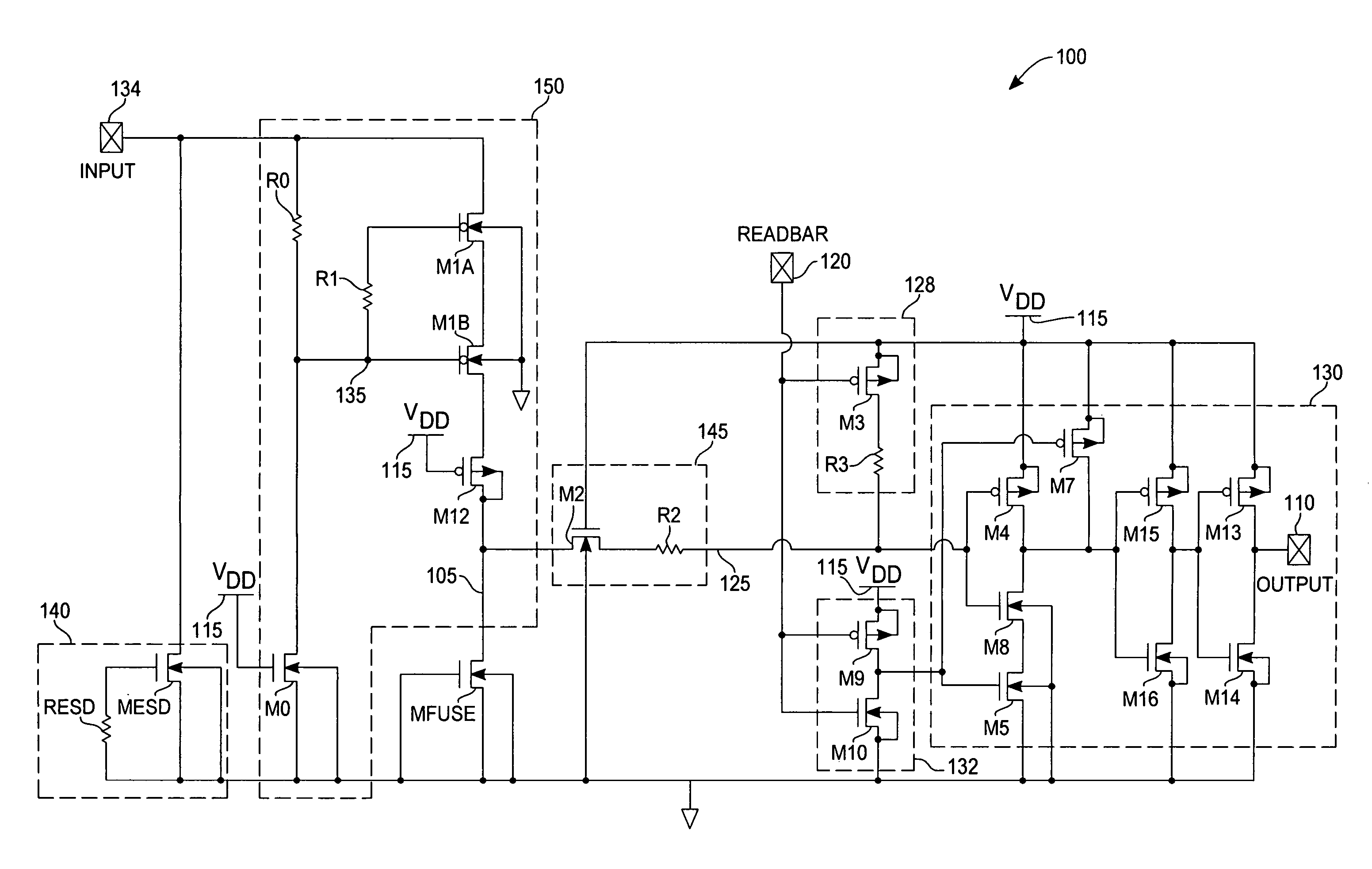
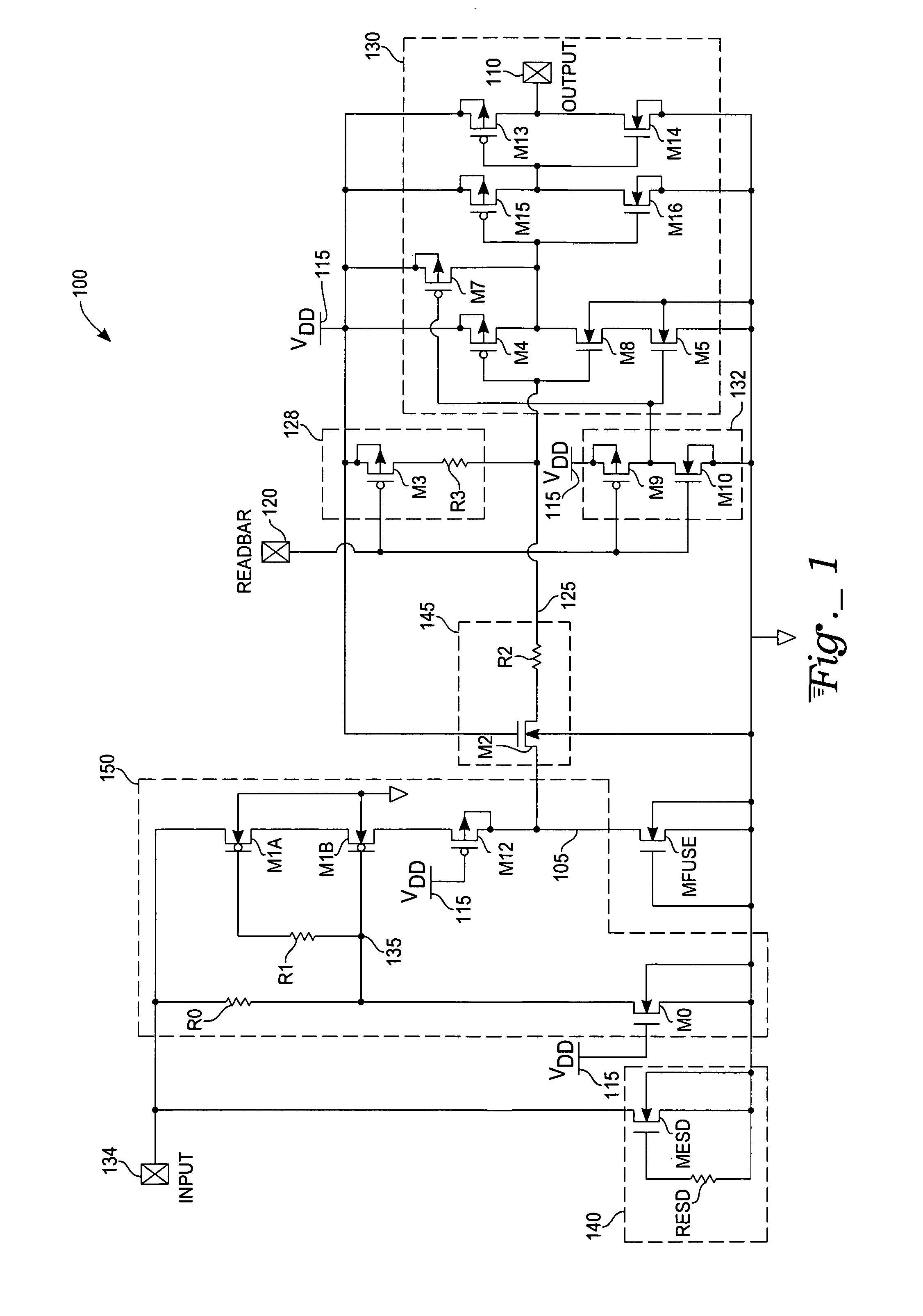
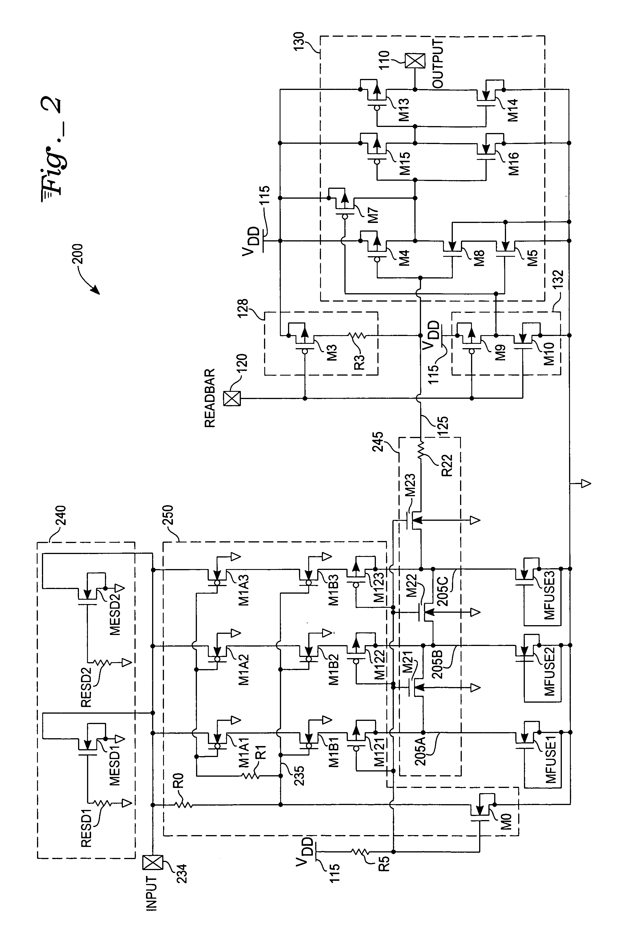
[0009]With reference to FIG. 1, an exemplary antifuse programming, protection, and sensing device contains an antifuse MFUSE. The antifuse MFUSE is a thin oxide NMOS transistor. The antifuse MFUSE is fabricated with a gate node, a source node, and a body node tied to ground level so that a conduction path through the antifuse MFUSE, from a drain node to ground, is highly resistive. In this configuration the antifuse MFUSE is considered an open circuit.

[0010]The antifuse MFUSE is connected between a VFUSE node 105 and ground. With a sufficiently high voltage applied to a drain of the antifuse MFUSE, it is damaged (blown) producing a low resistance path from the drain of the VFUSE node 105 to ground. In this state the antifuse MFUSE can be considered a short circuit.

[0011]A sense amplifier 130, containing a NAND gate structure M4, M8, M5, and M7 and a buffer M15, M16, M13, and M14, is used to sense the antifuse MFUSE and determine if it has been blown or not. An OUTPUT pad 110 communi...


PUM


Abstract

An antifuse programming, protection, and sensing device incorporates a control circuit to program and protect an antifuse. The antifuse, which is initially constructed as a low conductivity path, is programmable to a high conductivity path by application of an elevated voltage across terminals of the antifuse. Application of 0 volts to the VDD node of a conduction control portion of the antifuse programming, protection, and sensing device allows an elevated voltage for programming to be applied to the antifuse. Upon application of a nominal working voltage to the VDD node of the conduction control circuitry, the antifuse and an adjoining sense amplifier circuit are protected from overvoltage and tampering. The sense amplifier supplies a sense current to the antifuse, measures a voltage at an input to the antifuse, and determines a programmed state if a measured voltage level is low.

Description

TECHNICAL FIELD[0001]The present invention relates to a control circuit for antifuse technology. In particular, the present invention relates to a programming, protection, and sensing device for an antifuse cell.BACKGROUND ART[0002]Antifuses are used in integrated circuits to provide various circuit selection and configuration functions. When fabricated in a MOS technology, analog components, such as comparators or amplifiers, for example, may require an adjustment of operating parameters. Antifuses are used to select device configurations to effect parameter value adjustments.[0003]The antifuse is blown by applying a higher than normal voltage or laser beam to the antifuse. The high voltage, for example, produces a short circuit where an open circuit once existed. The application of the laser beam creates a similar short circuit condition. The blown antifuse alters a high impedance situation to a current conducting path that effects a change in a logic level with an applied current...

Claims


Application Information

Patent Timeline
Patent Type & Authority Patents(United States)
IPC IPC(8): H01H85/00
CPCG11C17/18
Inventor WICH, MATHEW T.GOSMAIN, VINCENT
Owner ATMEL CORP
Why Eureka
Try Eureka