Connector for making electrical contact at semiconductor scales

a technology of electrical connections and semiconductor devices, which is applied in the direction of electrical connection formation of printed elements, coupling device connections, instruments, etc., can solve the problems of prohibitively difficult and very expensive to use conventional techniques to make separable electrical connections to these semiconductor devices, and the difficulty of assembling lga packages onto pc boards or multi-chip modules, etc. problem, to achieve the effect of increasing the criticality

Inactive Publication Date: 2007-07-17
NEOCONIX INC
View PDF182 Cites 54 Cited by
  • Summary
  • Abstract
  • Description
  • Claims
  • Application Information

AI Technical Summary

Benefits of technology

[0017]According to one embodiment of the present invention, a connector for electrically connecting to pads formed on a semiconductor device includes a substrate and an array of contact elements of conductive material formed on the substrate. Each contact element includes a base portion attached to the top surface of the substrate and a curved spring portion extending from the base portion and having a distal end projecting above the substrate. The curved spring portion is formed to curve away from a plane of contact and has a curvature disposed to provide a controlled wiping action when engaging a respective pad of the semiconductor device.

Problems solved by technology

However, LGA packages are typically more difficult to assemble onto a PC board or a multi-chip module.
At the 250-micron pitch level, it is prohibitively difficult and very expensive to use conventional techniques to make separable electrical connections to these semiconductor devices.
The problem is becoming even more critical as the pitch of contact pads on a semiconductor device decreases below 50 microns and simultaneous connection to multiple contact pads in an array is required.
However, when conventional approaches are used to make electrical contact to solder balls, the solder balls may be damaged or completely dislodged from the package. FIG. 2A illustrates a contact element being applied to contact a solder ball.
The presence of such a void can affect the electrical characteristics of the connection and more importantly, degrades the reliability of the connection.
Another problem encountered by electrical connectors is the variation in coplanarity and positional misalignment of the contact points of a semiconductor device to be connected.
Although Eldridge discloses a approach for providing an array of all-metal contacts at semiconductor scales, the contact elements requires an expensive serial manufacturing process where the contact elements are formed one at a time.
Also, the inherent pointy shape of the contact structures results in piercing action which is prone to damaging the contact point such as a solder ball when making contact.
However, the metal springs point into the surface of the plane to be contacted and therefore is prone to damaging the solder balls when used to probe solder balls.
Khoury's approach provides an array of all-metal contacts at semiconductor scales but provides a limited amount of wiping action when interfacing with metal pads because the contacting component is parallel to the metal pad.
However, it will be obvious to one skilled in the art that such approaches can provide a wiping distance of only 10% or less of the overall dimension of the contact which is often not enough for a satisfactory electrical connection.
Such contact can lead to damage on the base surface of the solder ball which in turn can lead to void formation during subsequent solder reflow as shown in FIG. 2C.
In summary, the conventional connectors are not satisfactory for use with small pitch size semiconductor devices.
The conventional connects are also not satisfactory for providing wiping / piercing action without damaging the contact points such as the base surface of a solder ball.

Method used


Image

  • Connector for making electrical contact at semiconductor scales
  • Connector for making electrical contact at semiconductor scales
  • Connector for making electrical contact at semiconductor scales

Examples


Embodiment Construction

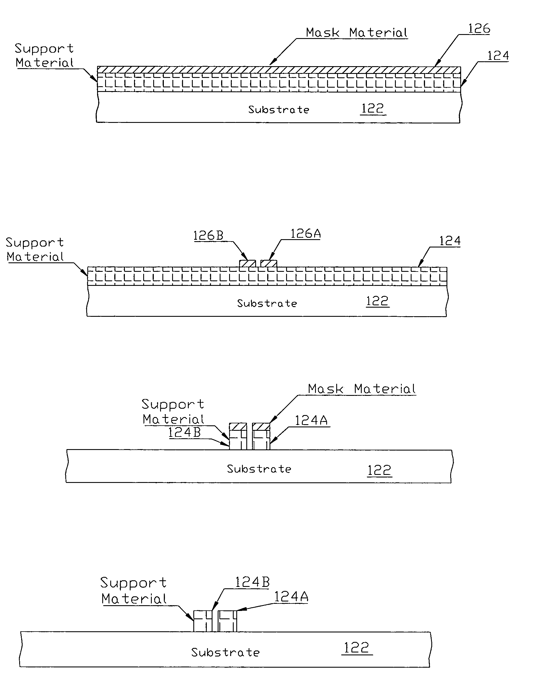
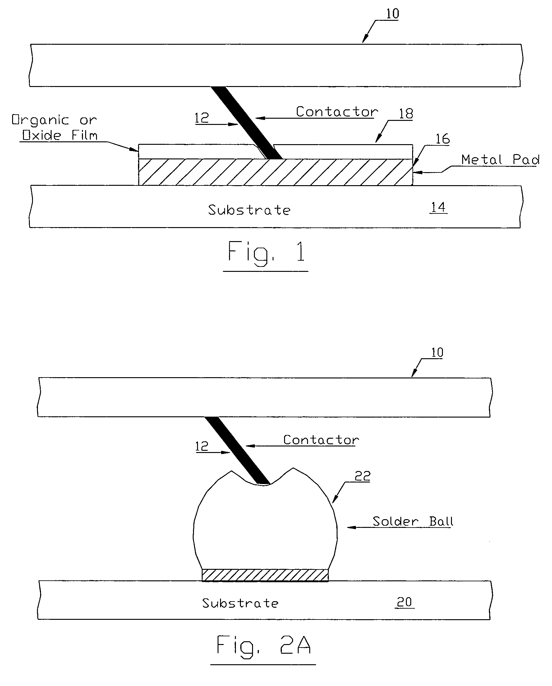
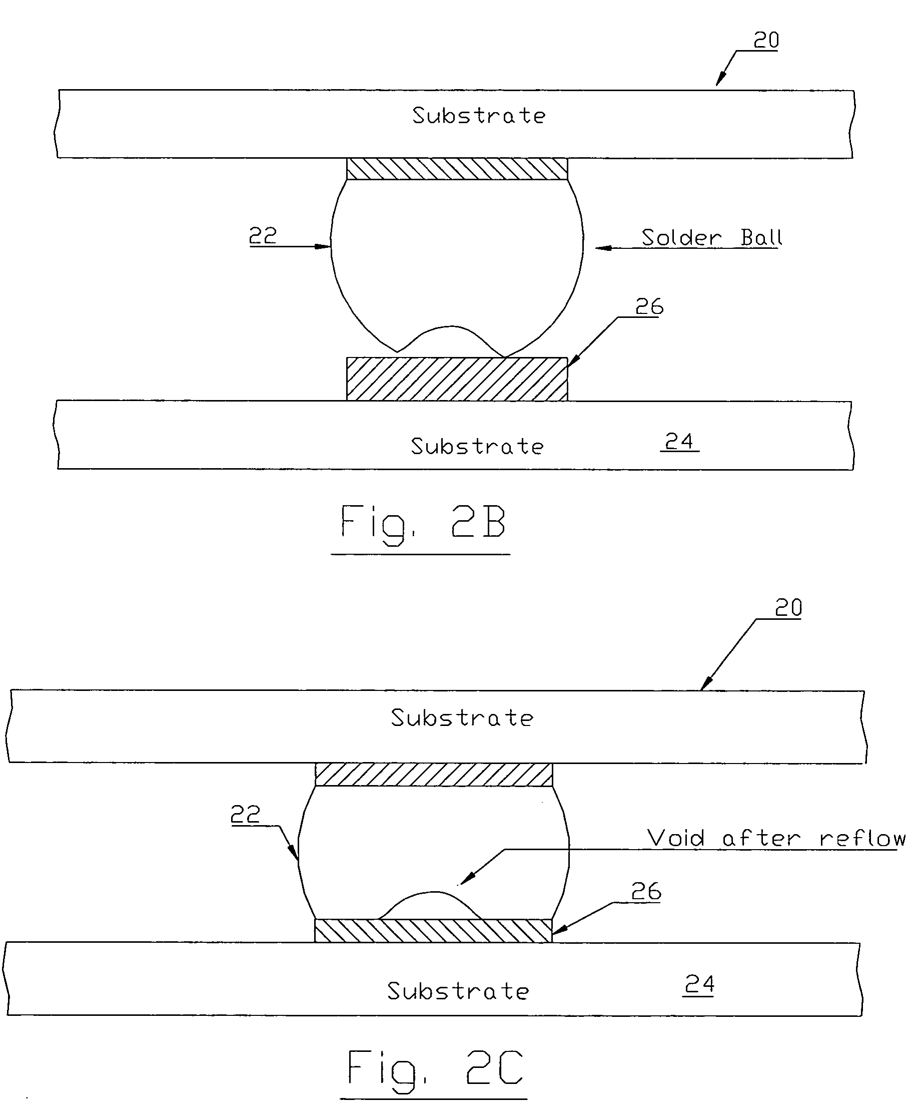
[0038]In accordance with the principles of the present invention, a connector for providing separable and remountable connection to a device includes an array of contact elements formed on a substrate where each contact element includes a curved spring portion formed to curve away from a plane of contact and having a curvature disposed to provide a controlled wiping action when engaging a contact point of the device. The connector of the present invention can be used to make electrical connection to devices at semiconductor scales, such as a silicon wafer or a packaged integrated circuit. The contact elements can be formed to make electrical connection to contact points having a pitch of 250 micron or less and in particular, the contact elements of the present invention enable electrical connection to contact points having a pitch of 50 micron or less. By providing a controlled wiping action, the connector of the present invention can be used to connect to a variety of contact surfa...


PUM


Abstract

A connector for electrically connecting to pads formed on a semiconductor device includes a substrate and an array of contact elements of conductive material formed on the substrate. Each contact element includes a base portion attached to the top surface of the substrate and a curved spring portion extending from the base portion and having a distal end projecting above the substrate. The curved spring portion is formed to curve away from a plane of contact and has a curvature disposed to provide a controlled wiping action when engaging a respective pad of the semiconductor device.

Description

CROSS-REFERENCE TO RELATED APPLICATIONS[0001]This application is related to concurrently filed and commonly assigned U.S. patent application Ser. No. 10 / 731,213, entitled “Method for Forming MEMS Grid Array Connector,” of Dirk D. Brown et al. The aforementioned patent application is incorporated herein by reference in its entirety.FIELD OF THE INVENTION[0002]The invention relates to reconnectable, remountable electrical connectors, and, in particular, to an electrical connector for connecting to semiconductor scale devices.DESCRIPTION OF THE RELATED ART[0003]Electrical interconnects or connectors are used to connect two or more electronic components together or to connect an electronic component to a piece of electrical equipment, such as a computer, router, or tester. For instance, an electrical interconnect is used to connect an electronic component, such as an integrated circuit (an IC or a chip), to a printed circuit broad. An electrical interconnect is also used during integrat...

Claims


Application Information

Patent Timeline
Patent Type & Authority Patents(United States)
IPC IPC(8): H01R12/00G01R1/04G01R1/067G01R3/00H01L23/32H01L23/48H01R12/04H01R12/71H01R13/03H01R13/24H01R43/00H01R43/20H05K3/32H05K3/40H05K7/10
CPCH01L24/72H01R13/03H01R13/2407H01R13/2442H05K3/4092H05K7/1069H01R12/52H01R12/714G01R1/0416G01R3/00H01L23/32H01L2924/01004H01L2924/01005H01L2924/01013H01L2924/01015H01L2924/01016H01L2924/01029H01L2924/01033H01L2924/01074H01L2924/01078H01L2924/01079H01L2924/01082H01L2924/01327H01L2924/14H01L2924/19041H01L2924/19042H01L2924/30107H01L2924/3011H01R43/007H01R43/205H05K3/326H01L2924/01006H01L2924/01019H01L2924/10253H01L2924/00
Inventor BROWN, DIRK D.WILLIAMS, JOHN D.RADZA, ERIC M.
Owner NEOCONIX INC
Why Eureka
Try Eureka