Optical interconnection module and method of manufacturing the same

a technology of optical interconnection module and optical waveguide, which is applied in the direction of optical waveguide light guide, optical elements, instruments, etc., can solve the problems of thermal dissipation, a big challenge for vertical coupling of light on the circuit board, and the limit of the speed of today's electronic system to a few ghz, so as to prevent the loss of coupling from the light source to the optical waveguide completely.

Inactive Publication Date: 2007-07-24
DOOSAN CORP
View PDF22 Cites 14 Cited by
  • Summary
  • Abstract
  • Description
  • Claims
  • Application Information

AI Technical Summary

Benefits of technology

[0015]Accordingly, the present invention has been made keeping in mind the above problems occurring in the previous art, and the objective of present invention is to provide an optical interconnection module having an optical waveguide. The optical waveguide embodies a reflecting mirror surface which is formed at an end of the optical waveguide, utilizing the total internal reflection of an ellipse; hence not only are the incoming waves totally reflected but also focused, at the same time, to the core of optical waveguide. If the light source is located at one focal point of the ellipse and the core of waveguide is centered at the other focal point of the ellipse, with the body of waveguide aligned with the direction of the light reflected from the mirror surface, the coupling loss from the light source to the optical waveguide can be completely prevented.

Problems solved by technology

However, as the amount of information is getting larger and transmission speed dramatically increases, electrical problems, such as skew in clock signals and electromagnetic interference (EMI), restrict speed of today's electronic systems to the limit of a few GHz.
Furthermore, thermal dissipation is another big problem in high speed electronic systems.
However, vertical coupling of light on circuit board is a big challenge in routing optical signals, on the basis that most of opto-electronic components are packaged as a form of surface-mounted device.
However, a conventional 45° reflection mirror surface or the curved reflecting mirror surface disclosed in FIG. 1 has a problem in that light incoming from a light source unit 30 is not totally reflected and some rays of the light leak out of the optical waveguide, thus causing loss.
Furthermore, the two mirror surfaces, 45° reflection mirror and circularly curved mirror, can not focus incoming rays 3-dimensionally into the core, leading to light leakages in a lateral direction (the direction from the right side to the left side of the optical waveguide), because even the circularly curved mirror (a piece of cylindrical surface) has a two-dimensionally varying shape.

Method used


Image

  • Optical interconnection module and method of manufacturing the same
  • Optical interconnection module and method of manufacturing the same
  • Optical interconnection module and method of manufacturing the same

Examples


Embodiment Construction

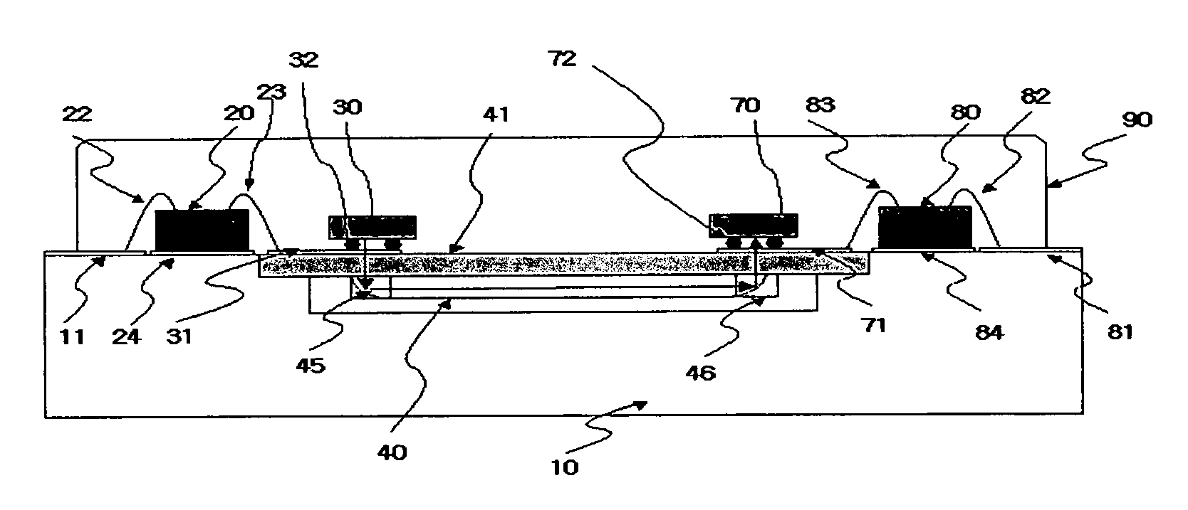
[0055]Reference now should be made to the drawings, in which the same reference numerals are used throughout the different drawings to designate the same or similar components.

[0056]The present invention is described in more detail with reference to the accompanying drawings in conjunction with embodiments illustrated in the drawings.

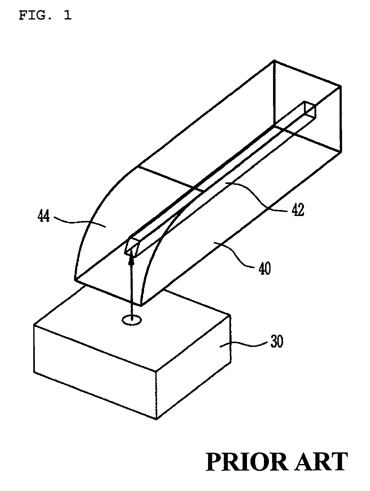
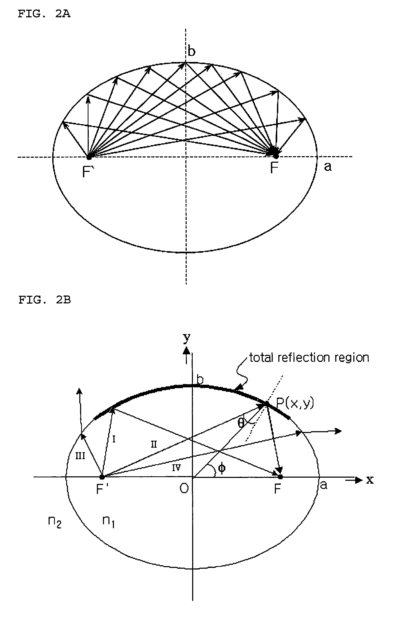
[0057]FIG. 2A is a diagram illustrating the reflection characteristics of an ellipse that is employed in the structure of a reflecting mirror surface that is applied to an end of the optical waveguide of the present invention. FIG. 2B is a diagram illustrating a region that satisfies a total reflection condition.

[0058]In FIG. 2A, if the boundary of an ellipse is a mirror surface, all of the rays of light emitted from one focal point F′ are reflected by the boundary of the ellipse and gather at the other focal point F.

[0059]Even if the boundary of the ellipse is not a mirror surface but is a surface made of a material having a reflective index n1, a regi...


PUM


Abstract

The present invention relates generally to an optical interconnection module for vertical optical coupling and a method of manufacturing the optical interconnection module. The optical interconnection module includes an optical waveguide. The optical waveguide includes substrate on which electrode pads and a predetermined circuit pattern are formed; a light source unit provided on the substrate and configured to generate an optical signal and emit the signal to an outside; an optical detection unit for receiving the optical signal from the light source unit and converting the optical signal into an electric signal; drive units provided on the substrate and configured to drive the light source unit and the light detection unit in response to electric signals supplied through the electrode pads; and a cladding layer, a core layer layered on the cladding layer, and an elliptical reflecting mirror surface placed on an end of the core layer facing the light source unit.

Description

BACKGROUND OF THE INVENTION[0001]1. Field of the Invention[0002]The present invention relates generally to an optical interconnection module for vertical optical coupling and a method of manufacturing the optical interconnection module.[0003]2. Description of the Related Art[0004]In the majority of electronic systems, the electrical connections between circuit boards, chips or systems are implemented using a metallic wire. However, as the amount of information is getting larger and transmission speed dramatically increases, electrical problems, such as skew in clock signals and electromagnetic interference (EMI), restrict speed of today's electronic systems to the limit of a few GHz. Furthermore, thermal dissipation is another big problem in high speed electronic systems. To overcome such problems, optical interconnection is introduced into circuit board level. Optical interconnection has great advantage over electronic wiring, not causing any EMI and thermal problems. However, vert...

Claims


Application Information

Patent Timeline
Patent Type & Authority Patents(United States)
IPC IPC(8): G02B6/26G02B6/36G02B6/42
CPCG02B6/10G02B6/4214H01L2224/48091H01L2224/73265H01L2924/00014H01L2924/3011H01L2924/00G02B6/26G02B6/42
Inventor JEON, KEUM SOOLEE, MIN SUKANG, SUNG HOKIM, YONG WOOKPARK, IN SU
Owner DOOSAN CORP
Why Eureka
Try Eureka