Method for optimizing high frequency performance of via structures

Active Publication Date: 2007-07-24
SANMINA-SCI CORPORATION
View PDF6 Cites 55 Cited by
  • Summary
  • Abstract
  • Description
  • Claims
  • Application Information

AI Technical Summary

Benefits of technology

[0014]Finally, the S-parameters of the via structure after optimization may be calculated to verify the optimization results. The present invention allows for constraints

Problems solved by technology

At higher transmission data rates, resistance, dielectric absorption, and radiation losses, cross-talk, and structural resonances of passive interconnects can significantly degrade the quality of signals propagatin

Method used


Image

  • Method for optimizing high frequency performance of via structures
  • Method for optimizing high frequency performance of via structures
  • Method for optimizing high frequency performance of via structures

Examples


Example

[0023]Repeat use of reference characters throughout the present specification and appended drawings is intended to represent the same or analogous features or elements of the invention.

DETAILED DESCRIPTION OF THE PREFERRED EMBODIMENTS

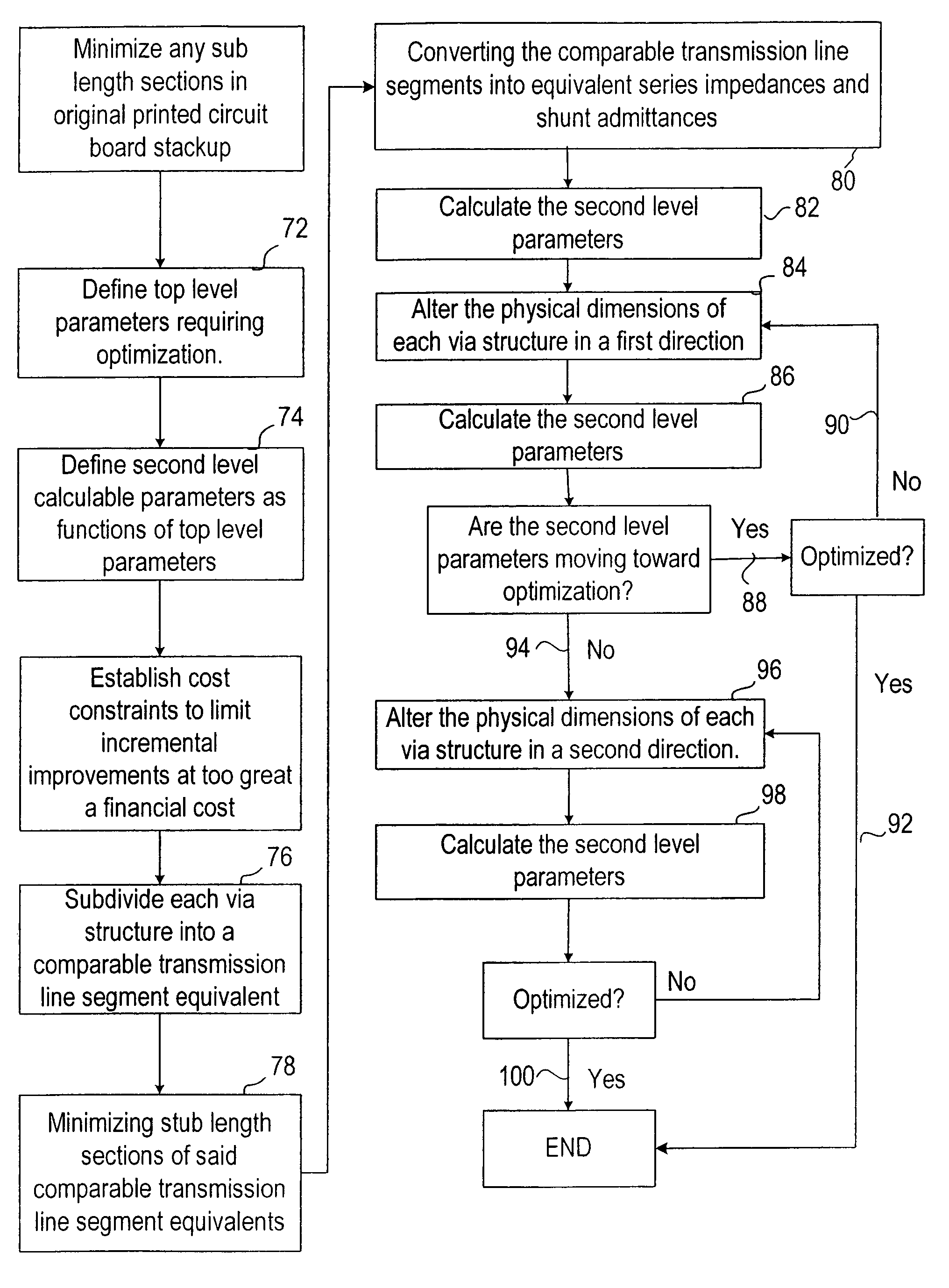
[0024]Reference will now be made in detail to presently preferred embodiments of the invention, examples of which are fully represented in the accompanying drawings. Such examples are provided by way of an explanation of the invention, not limitation thereof. In fact, it will be apparent to those skilled in the art that various modifications and variations can be made in the present invention, without departing from the spirit and scope thereof. For instance, features illustrated or described as part of one embodiment can be used on another embodiment to yield a still further embodiment. Still further, variations in selection of materials and / or characteristics may be practiced, to satisfy particular desired user criteria. Thus, it is intended that the ...


PUM


Abstract

A method for enhancing the high frequency signal integrity performance of a printed circuit board (PCB) or backplane is provided. According to one embodiment of the present invention, the method involves the use of S-parameters as the primary cost factors associated with an iterative process to optimize the physical dimensions and shape of a single or a collection of vias within the PCB or backplane. In certain embodiments, the process involves the representation of the via components as equivalent lumped series admittances and impedances, as well as, RLGC sub-circuits upon which basic circuit analysis is performed to optimize secondary characteristics, for example, the maximization of the sub-circuit's resistance and/or the minimization of the sub-circuit's capacitance. The iterative process involves the alteration of physical dimensions and the shape of the via components such that the secondary characteristics are optimized.

Description

BACKGROUND OF THE INVENTION[0001]This invention generally relates to a method for assuring enhanced signal integrity in various electronic components operating at higher frequencies. In particular, the present invention relates to a method for optimizing via structures in such components. More particularly, the present invention relates to a method for optimizing via structures for the enhanced high frequency performance of printed circuit boards and backplanes.[0002]Today's electronic products, including computers, cellular telephones, and networking systems operate at ever increasing transmission data rates. At higher transmission data rates, resistance, dielectric absorption, and radiation losses, cross-talk, and structural resonances of passive interconnects can significantly degrade the quality of signals propagating through the interconnect. One of the primary circuit elements that attenuates and distorts analog, radio frequency and digital signals is the via. Via signal degra...

Claims


Application Information

Patent Timeline
IPC IPC(8): H03K17/693H01L23/02H02B1/00G06F17/50H05K1/02H05K1/11H05K3/00
CPCG06F17/5036H05K3/0005H05K1/023H05K1/0237H05K1/115H05K2203/163G06F30/367
Inventor GISIN, FRANZPANOS, WILLIAMKHANDOKAR, MAHAMUD
Owner SANMINA-SCI CORPORATION
Why Eureka
Try Eureka