Semiconductor package with a flip chip on a solder-resist leadframe

a technology of resisting leadframes and semiconductors, which is applied in the direction of semiconductor devices, semiconductor/solid-state device details, electrical apparatus, etc., can solve the problems of affecting the sealing effect the sensitivity of the soldering mask, so as to achieve the effect of effectively limiting the soldering area of a plurality of bumps, avoiding solder contamination and bump collapse, and improving mold locking ability

Active Publication Date: 2007-08-07
ADVANCED SEMICON ENG INC
View PDF5 Cites 24 Cited by
  • Summary
  • Abstract
  • Description
  • Claims
  • Application Information

AI Technical Summary

Benefits of technology

[0004]It is a primary object of the present invention to provide a semiconductor package with a flip chip on a leadframe to avoid solder contamination and bump collapse. Leads of the leadframe have a plurality of bump-bonding regions at fan-in ends thereof, and a plurality of outer connecting regions at fan-out ends thereof. A plurality of indentations are formed at the upper surfaces and adjacent to bump-bonding regions at the fan-in ends of the leads in replacement of well-known solder mask on a leadframe. The bumps of the flip chip will not excessively wet and spread on the leads. Preferably, the indentations can be filled with a molding compound to firmly fix the fan-in ends of the leads. Also a leadframe for the semiconductor package is disclosed.
[0005]It is a secondary object of the present invention to provide a semiconductor package with a flip chip on a leadframe. It utilizes the indentations at the upper surfaces of the leads of the leadframe to define a plurality of bump-bonding regions. Preferably, the indentations have a reversed “Ω”-shaped profile for effectively limiting soldering area of a plurality of bumps on the flip chip. The bumps can be bonded to the bump-bonding regions of the leads without excessive diffusion during a reflowing process.
[0006]It is another object of the present invention to provide a semiconductor package with a flip chip on a leadframe with better mold locking capability. The leads of the leadframe have a plurality of recessions in the lower surfaces thereof. The recessions are formed between the indentations and the outer connecting regions, which can be filled with a molding compound for firmly fixing the leads.
[0007]In accordance with the present invention, a semiconductor package generally includes a plurality of leads from a leadframe, a flip chip and a molding compound. Each lead has an upper surface and a lower surface. The upper surfaces include a plurality of bump-bonding regions at the fan-in ends of the leads. The lower surfaces include a plurality of outer connecting regions at the fan-out ends of the leads. The leads have a plurality of indentations at the upper surfaces and adjacent to the corresponding bump-bonding regions to define the soldering area of the bump-bonding regions. The flip chip is located on the leads by connecting a plurality of bumps of the flip chip to the bump-bonding regions of the leads. The molding compound encapsulates the flip chip and the leads, but the outer connecting regions of the leads are exposed out of the molding compound. Preferably, the indentations have a reversed “Ω”-shaped profile and are filled with the molding compound to improve the mold locking capability and the stop effect of solder diffusion. In various embodiments, parts of the leads include the fan-in ends may are formed on an upset, or a plurality of recessions are formed in the lower surfaces between the indentations and the outer connecting regions, so as to improve mold locking capability of the leads within the molding compound.

Problems solved by technology

However, the leadframe provided for flip-chip connection is slightly different from conventional leadframe for wire-bonding connection.
However the bumps will easily wet other portions of the leads during reflowing process.
When the solder mask is printed on the upper surfaces of the leads, the consumption of solder mask is very large because that the thickness of the leads is much thicker than that of the well-known traces of a substrate.
Moreover, since there is no supporting resin layer below the leads, a solder mask is hard to form and easily contaminates the leadframe and processing machine.
Furthermore, the bonding strength between the leads coated with solder masked and the molding compound is weak.
As a result, the leads are easily delaminated from the molding compound and short circuit occurs.

Method used


Image

  • Semiconductor package with a flip chip on a solder-resist leadframe
  • Semiconductor package with a flip chip on a solder-resist leadframe
  • Semiconductor package with a flip chip on a solder-resist leadframe

Examples


first embodiment

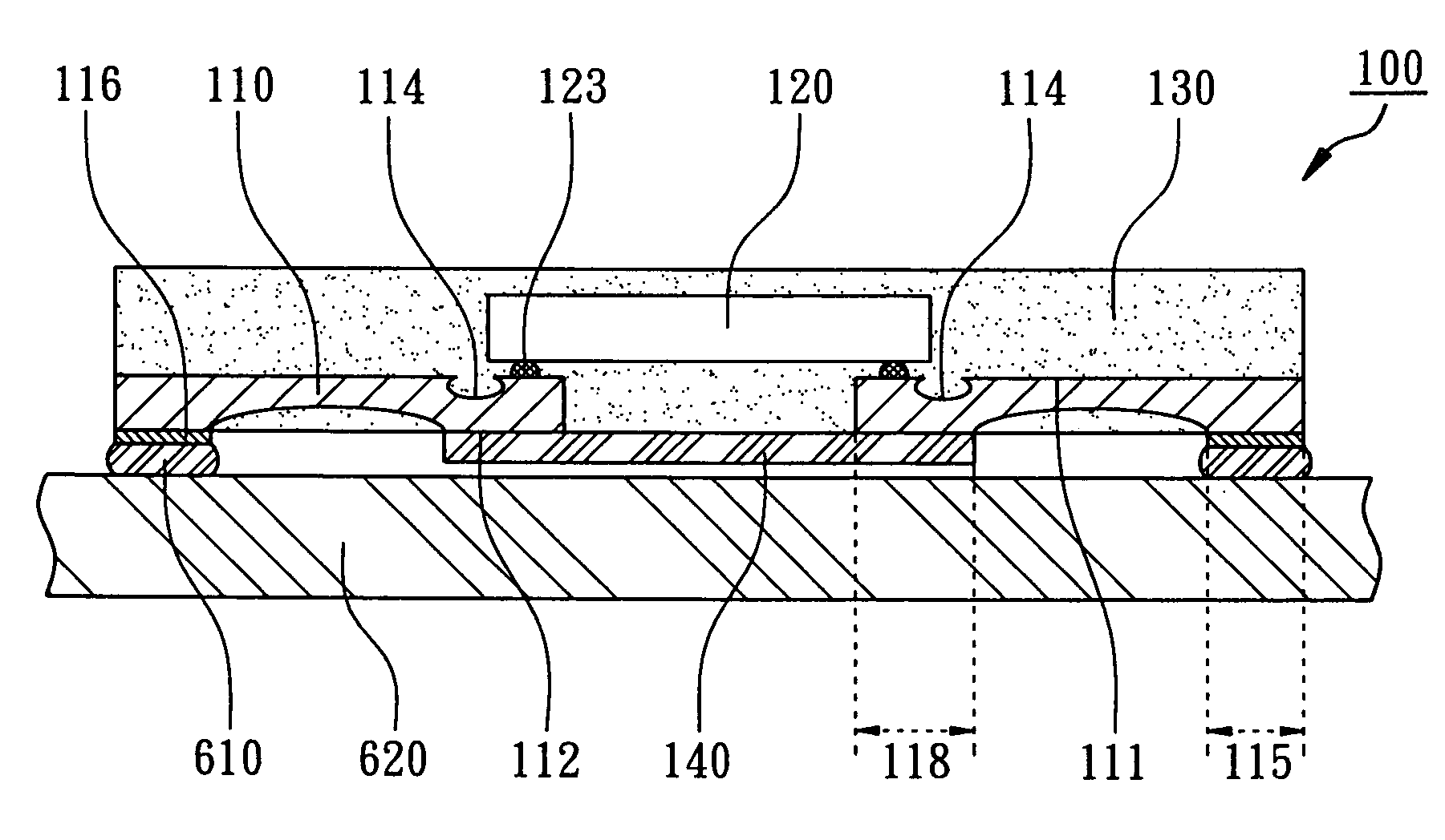
[0015]the present invention discloses a semiconductor package with a flip chip on a leadframe. Referring to FIG. 1, the semiconductor package 100 mainly includes a plurality of leads 110, a flip chip 120 and a molding compound 130. The leads 110 are parts of a leadframe which is made of copper, iron or its alloy, such as leadframe for QFN (Quad Flat Non-leaded) packages or SON (Small Outline Non-leaded) packages. The leads 110 according to various types may be designed to arrange on four sides or two sides on the bottom surface of the molding compound 130. Each lead 110 has an upper surface 111 and a lower surface 112. In this embodiment, the leads 110 have a fan-out design and extend to an appropriate length preferably more than about 600 μm approximately, but there is no outer lead extending from the molding compound 130. The upper surfaces 111 of the leads 110 include a plurality of bump-bonding regions 113 at the fan-in ends of the leads 110 for soldering connection of a plurali...

second embodiment

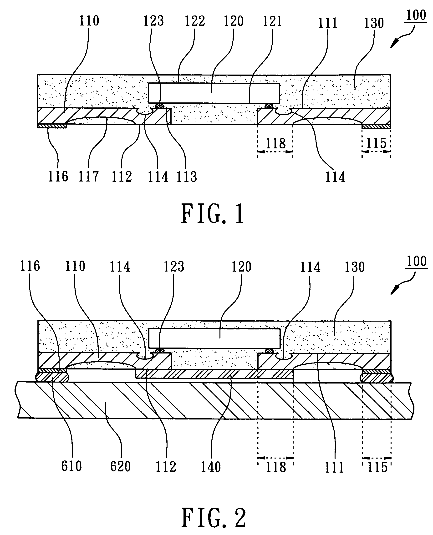
[0019]the present invention discloses another semiconductor package with a flip chip on a leadframe. Referring to FIG. 3, the semiconductor package 200 generally includes a plurality of leads 210, a flip chip 220 and a molding compound 230. The flip chip 220 is mounted on the leads 210 and encapsulated by the molding compound 230. Each lead 210 has an upper surface 211 and a lower surface 212. A plurality of bump-bonding regions 213 are formed on the upper surfaces 211 and at the fan-in ends of the lead 210, and are defined by a plurality of adjacent indentations 214. The indentations 214 preferably have a reversed “Ω”-shaped profile to prevent the bumps 222 on the active surface 221 of the chip 220 from excessively wetting and diffusion. The indentations 214 can be filled with the molding compound 230. The leads 210 are bended to allow the fan-in ends including the bump-bonding regions 213 are formed on an upset 216 for flip chip mounting of the flip chip 220. The lower surfaces 21...


PUM


Abstract

A semiconductor package includes a flip chip mounted on a plurality of leads and encapsulated by a molding compound. The upper surfaces of the leads includes a plurality of bump-bonding regions at the fan-in ends of the leads, and the lower surfaces of the leads include a plurality of outer connecting regions at the fan-out ends of the leads. A plurality of indentations are formed at the upper surfaces of the leads and adjacent to the corresponding bump-bonding regions so as to avoid solder contamination on the leads. After molding, the indentations are filled with the molding compound. Preferably, the indentations have a reversed “Ω”-shaped profile to prevent bumps of the flip chip from excessively wetting over the other portions of the leads to firmly fix the fan-in ends of the leads.

Description

FIELD OF THE INVENTION[0001]The present invention relates to a semiconductor package, more particularly to a semiconductor package with a flip chip on a leadframe.BACKGROUND OF THE INVENTION[0002]According to various requirements from customers, known semiconductor packages have various package configurations. One type of semiconductor packages is that a flip chip is mounted on a leadframe. There are a plurality of bumps formed on active surface of a flip chip to connect a plurality of leads in replacement of bonding wires for inner electrical connection within a molding compound. However, the leadframe provided for flip-chip connection is slightly different from conventional leadframe for wire-bonding connection. The leadframe has a plurality of appropriate bump-bonding regions at the fan-in end of leads corresponding to the bumps of the flip chip. However the bumps will easily wet other portions of the leads during reflowing process.[0003]Flip-chip typed QFN packages (Quad Flat No...

Claims


Application Information

Patent Timeline
Patent Type & Authority Patents(United States)
IPC IPC(8): H01L23/48H01L23/31H01L23/433H01L23/495
CPCH01L23/3107H01L23/49548H01L23/49558H01L23/49575H01L24/17H01L23/4334H01L2224/32145H01L2224/13099H01L2224/16245H01L2224/48091H01L2224/48247H01L2224/73253H01L2224/73265H01L2924/01029H01L2924/01079H01L2924/01082H01L2924/16152H01L2924/07802H01L2224/45144H01L2924/014H01L2924/01033H01L2924/01006H01L24/48H01L2924/00014H01L2924/00H01L24/45H01L2924/14H01L2924/181H01L2924/00012
Inventor LIU, CHIENWANG, HSUEH-TEWANG, MENG-JENCHIU, CHI-HAOHUANG, TAI-YUAN
Owner ADVANCED SEMICON ENG INC
Why Eureka
Try Eureka