Techniques for providing EMI shielding within a circuit board component

a technology of circuit board and component, applied in the direction of magnetic/electric field screening, electrical apparatus contruction details, printed circuit non-printed electric components association, etc., can solve the problems of clip typically requiring additional space around the device package, clip consuming circuit board space, ground connection not, etc., to minimize the escape of electromagnetic interface

Active Publication Date: 2007-08-07
CISCO TECH INC
View PDF8 Cites 28 Cited by
  • Summary
  • Abstract
  • Description
  • Claims
  • Application Information

AI Technical Summary

Benefits of technology

[0010]In one arrangement, the heat spreader interface includes a conductive ground plane disposed along a flat surface of the substrate. The conductive ground plane completely encircles the die interface contiguously in a 360 degree manner to minimize escape of electromagnetic interface from the die during operation of the integrated circuitry. Since the conductive ground plane fully surrounds the die interface, there is thorough and robust EMI shielding of the die.
[0011]In another arrangement, the heat spreader interface includes conductive ground plates disposed along a flat surface of the substrate. The conductive ground plates encircle the die interface in a 360 degree manner to minimize escape of electromagnetic interface from the die during operation of the integrated circuitry. This arrangement provides EMI shielding in all directions around the die (i.e., 360 degrees) as well as enables traces (e.g., signal traces) to reside along the surface of the substrate.

Problems solved by technology

Unfortunately, there are deficiencies to the above-described approach to grounding the heat sink and the heat spreader using external metallic clips.
For example, such clips typically require additional space around the device package.
In particular, the clips consume circuit board space that could otherwise be used by other circuit board components.
The dedication of such space for additional ground connections not only consumes circuit board real estate, but also hinders routing of signal traces to and from the mounting location.
Accordingly, use of the metallic clips imposes significant restrictions in the area around the mounting location of the device package.
Additionally, the metallic clips are often difficult to remove due to their strength and rigidity.
Accordingly, if the manufacturer needs to remove the clips (e.g., to replace a damaged heat sink, to more thoroughly inspect the AAP device, etc.), the manufacturer often must break the clips and, in the process, risk damaging the AAP device and / or fracturing the solder joints connecting the AAP device to the circuit board.
As a result, in some situations, the use of external metallic clips creates more problems than it solves.
Furthermore, although the metallic clips are typically distributed around the AAP package (e.g., eight clips extending around the AAP package), the metallic clips typically do not do a thorough job as an EMI fence to shield neighboring components from EMI emanating from the die.
In particular, gaps between the clips typically allow EMI to easily escape thus allowing the EMI to then interfere with signals in the vicinity of the AAP device as well as make it more difficult for the AAP device to pass Federal Communications Commission (FCC) regulations.
Moreover, it will become more difficult to provide reliable thermal management and competent EMI control as the operating speeds and power consumption of circuit board devices increase over time.

Method used


Image

  • Techniques for providing EMI shielding within a circuit board component
  • Techniques for providing EMI shielding within a circuit board component
  • Techniques for providing EMI shielding within a circuit board component

Examples


Embodiment Construction

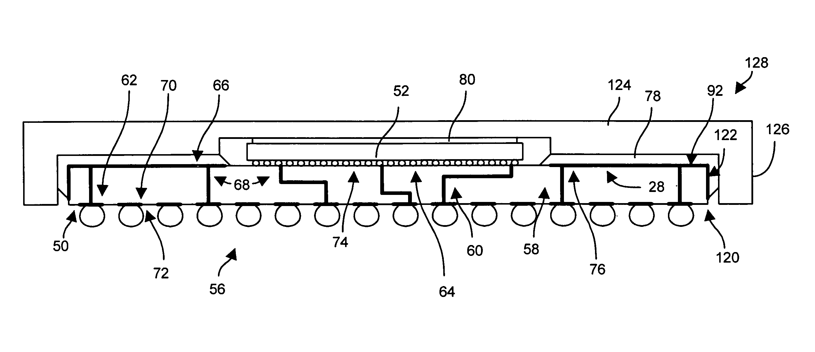
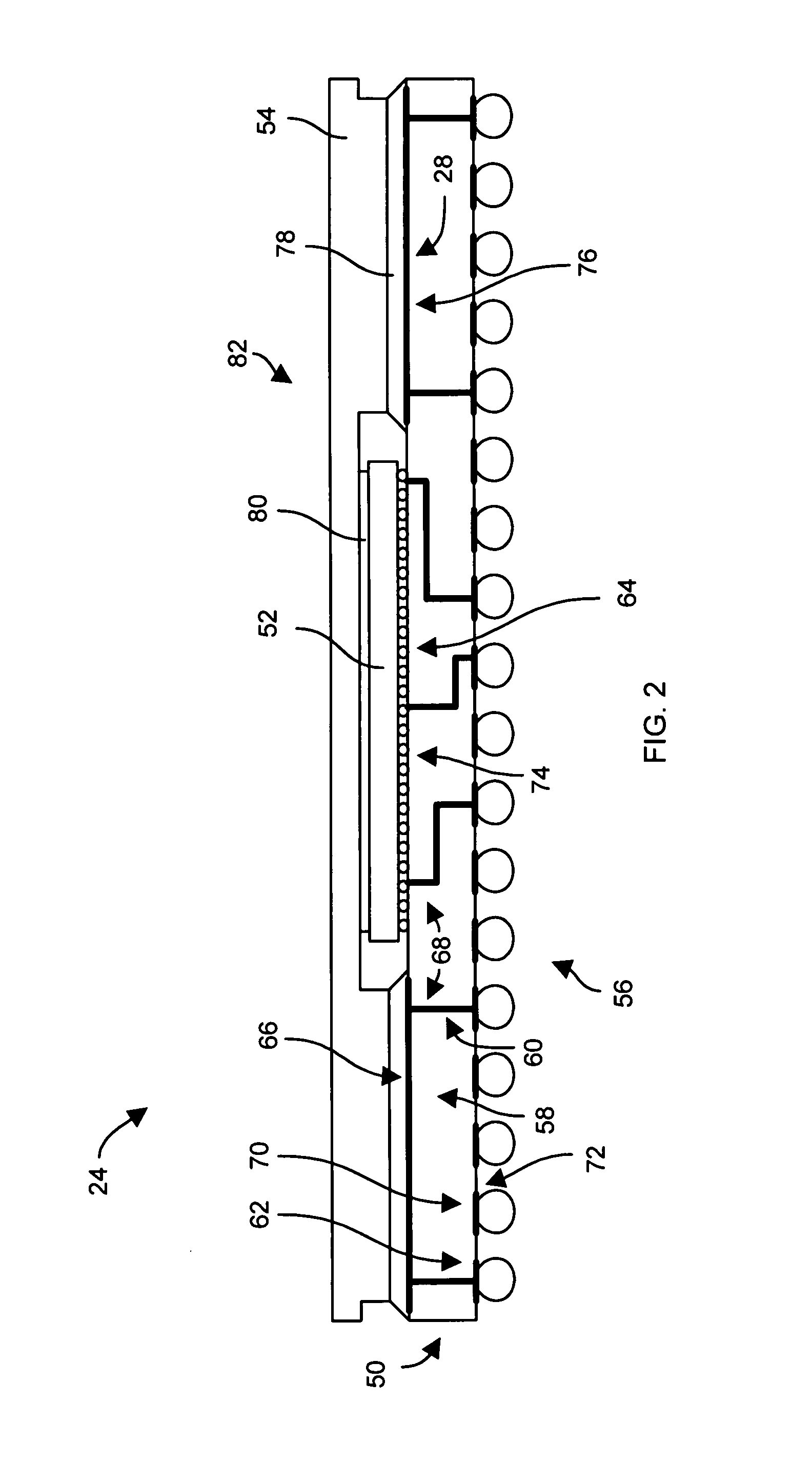
[0019]Embodiments of the invention are directed to electromagnetic interference (EMI) shielding techniques which utilize conductive material which is disposed around a circuit board component die but within the component itself. Such conductive material in combination with a heat spreader of the component is capable of forming an EMI shield internally within the component itself when connected to a ground reference of a circuit board through a circuit board interface of the component to block EMI which radiates from the die during operation. Accordingly, there is no need for external metallic clips to ground a heat sink and the heat spreader as in conventional EMI barrier approaches. Rather, the circuit board space around the device, which would otherwise be used by the metallic clips, is now available for use by other circuit board structures (e.g., signal traces, other circuit board components, etc.).

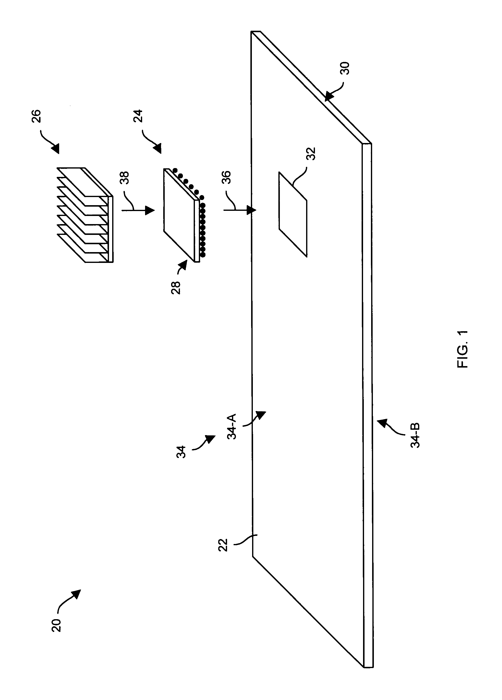
[0020]FIG. 1 shows an exploded view of a circuit board module (or motherboard) 20...


PUM


Abstract

A circuit board component includes a substrate having non-conductive material and conductive material supported by the non-conductive material. The conductive material defines a circuit board interface, a die interface, a heat spreader interface, and (iv) a set of connections which interconnects the circuit board interface, the die interface and the heat spreader interface. The component further includes a die coupled to the die interface. The die includes integrated circuitry which is configured to electrically communicate with a circuit board when the circuit board couples to the circuit board interface. The component further includes a heat spreader coupled to the heat spreader interface. The heat spreader is configured to dissipate heat from the die. The heat spreader in combination with the heat spreader interface forms an electromagnetic interference shield when a portion of the circuit board interface connects to a ground reference of the circuit board.

Description

BACKGROUND OF THE INVENTION[0001]A typical Area Array Package (AAP) device such as a Ceramic Column Grid Array (CCGA) device or a Ball Grid Array (BGA) device includes a substrate, a die and a heat spreader. The substrate includes layers of non-conductive material and conductive material sandwiched together into a substantially plane-shaped element which supports (i) an array of circuit board contacts on one side (e.g., columns, balls, etc.) for connecting to a circuit board, and (ii) die contacts on the other side for connecting to the die. The die is a silicon-based chip containing integrated circuitry which generates heat during operation. The heat spreader (or lid) typically glues to the side of the substrate having the die contacts (e.g., using a thermal adhesive) and extends over the die to physically protect the die. A thermally conductive but electrically non-conductive material (e.g., thermal grease) resides typically between the heat spreader and the die to convey heat fro...

Claims


Application Information

Patent Timeline
Patent Type & Authority Patents(United States)
IPC IPC(8): H05K7/20H01L23/34
CPCH01L23/3675H05K9/0039H01L23/552H01L23/49816H01L23/49822H01L2224/16225H01L2224/73253H01L2924/15311H01L2924/16251H01L2924/01322H01L2924/00
Inventor XUE, JIEYANG, ZHIPINGZOU, YIDA
Owner CISCO TECH INC
Why Eureka
Try Eureka