Static random access memory device and method of reducing standby current

a memory device and random access technology, applied in static storage, information storage, digital storage, etc., can solve the problems of increasing the total leakage current on standby, increasing the leakage current in the off-state, so as to reduce the leakage of standby

Inactive Publication Date: 2007-08-07
KK TOSHIBA
View PDF3 Cites 61 Cited by
  • Summary
  • Abstract
  • Description
  • Claims
  • Application Information

AI Technical Summary

Problems solved by technology

As regards SRAMs, a problem has become prominent in that leakage current increases in memory cells on standby, as a consequence of the reduced size and operation voltage of LSIs.
As a consequence, the leakage current tunneling through the gate oxide film (gate leakage) increases and thereby brings about an increase in the total leakage current on standby.
In addition, the threshold voltage of MOSFETs decreases along with decrease in the operation voltage of LSIs, which brings about an increase in the leakage current in the OFF-state (sub-threshold leakage).

Method used


Image

  • Static random access memory device and method of reducing standby current
  • Static random access memory device and method of reducing standby current
  • Static random access memory device and method of reducing standby current

Examples


first embodiment

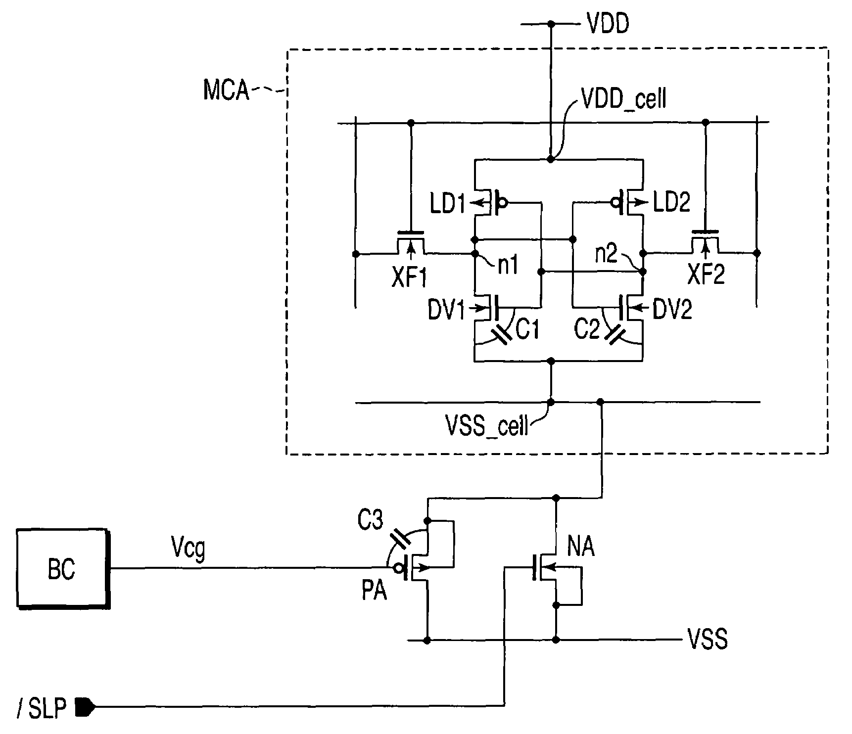
[0034]FIG. 4 is a block diagram showing an SRAM (semiconductor storage device) according to a first embodiment of the present invention. The SRAM includes a memory cell array 21, in which memory cells 24 are respectively disposed at addresses arrayed in a matrix format. Word lines WL for selecting the memory cells are respectively connected to the rows of the memory cell array 21. Complementary pairs of data lines BL and / BL for transmitting data to and from the memory cells are respectively connected to the columns of the memory cell array 21.

[0035]A row address buffer 11 and a row decoder 13 are disposed to select the word lines WL. A column address buffer 15 and a column decoder 17 are disposed to select the data lines BL and / BL. A sensing circuit 19 is connected to the data lines BL and / BL, for reading stored data. The row address buffer 11 and column address buffer 12 are connected to a control section CS1 for generating address signals, data signals, and so forth. The contro...

second embodiment

[0069]FIG. 9 is a view showing an SRAM (semiconductor storage device) according to a second embodiment of the present invention, focusing on circuitry for clamping the standby voltage thereof. In the device shown in FIG. 9, a potential line SL connected to a ground potential VSS is provided with two transistors N11 and N12 disposed thereon in parallel with each other, in place of the first additional transistor N1 shown in FIG. 6. Except for the matters relating to the two transistors N11 and N12, the device shown in FIG. 9 has the same structure as the device shown in FIG. 6.

[0070]More specifically, the transistors N11 and N12 are formed of NMISFETs, and typically NMOSFETs. The transistors N12 is set to have a smaller current driving ability than the transistor N11. The gate terminals of the transistors N11 and N12 are supplied with selection signals SEL11 and SEL12 through selection signal supply lines L11 and L12, respectively, to set the transistors N11 and N12 in the ON-state w...

third embodiment

[0075]FIG. 11 is a view showing an SRAM (semiconductor storage device) according to a third embodiment of the present invention, focusing on circuitry for clamping the standby voltage thereof. In the device shown in FIG. 11, a selection signal supply line L1 connected to the gate terminal of a transistor N1 is provided with an inverter circuit 60 disposed thereon, in place of the delay circuit 40 shown in FIG. 6. Except for the matters relating to the inverter circuit 60, the device shown in FIG. 11 has the same structure as the device shown in FIG. 6. Although the effects of the device shown in FIG. 11 are similar to those of the device shown in FIG. 9, the device shown in FIG. 11 can attain the same effect with a simpler circuit.

[0076]More specifically, the inverter circuit 60 includes a NOT gate 64, and a pull-up transistor N61 and a pull-down transistor N62 connected to the power supply potential VDD and the ground potential VSS, respectively. The transistors N61 and N62 are for...


PUM


Abstract

A semiconductor storage device includes first and second additional FETs disposed in parallel on one of potential lines for supplying first and second drive potentials to each SRAM memory cell. The gate terminal of the first additional FET is supplied with a selection signal through a selection signal supply line to turn on the first additional FET, when the memory cell is selected. The gate terminal of the second additional FET is supplied with a bias potential through a bias supply line, wherein the bias potential has first and second levels respectively corresponding to non-selection and selection of the memory cell.

Description

CROSS-REFERENCE TO RELATED APPLICATIONS[0001]This application is based upon and claims the benefit of priority from prior Japanese Patent Application No. 2005-152437, filed May 25, 2005, the entire contents of which are incorporated herein by reference.BACKGROUND OF THE INVENTION[0002]1. Field of the Invention[0003]The present invention relates to a semiconductor storage device, and particularly to a technique for reducing standby current in a static semiconductor storage device, e.g., an SRAM (SRAM: Static Random Access Memory).[0004]2. Description of the Related Art[0005]SRAMs (typically, each memory cell includes six transistors to store one bit) are widely used for LSIs (LSI: Large Scale Integrated circuit). As regards SRAMs, a problem has become prominent in that leakage current increases in memory cells on standby, as a consequence of the reduced size and operation voltage of LSIs. The term “standby” means that a memory cell is in the non-selected state.[0006]The thickness of ...

Claims


Application Information

Patent Timeline
Patent Type & Authority Patents(United States)
IPC IPC(8): G11C5/14
CPCG11C11/417
Inventor HIRABAYASHI, OSAMU
Owner KK TOSHIBA
Why Eureka
Try Eureka