Memory system having memory modules with different memory device loads

a memory module and memory device technology, applied in the field of memory systems, can solve the problems of signal distortion and signal modification, narrow bandwidth of the memory bus channel, and electrically deteriorating channel characteristics, and achieve the effects of improving signal integrity, increasing signal delay time, and prolonging the length of the signal transmission lin

Active Publication Date: 2007-08-07
SAMSUNG ELECTRONICS CO LTD
View PDF9 Cites 6 Cited by
  • Summary
  • Abstract
  • Description
  • Claims
  • Application Information

AI Technical Summary

Benefits of technology

[0010]The present invention is at least partially characterized by increasing the length of a transmission line of a first memory module relative to the length of a transmission line of a second memory module, where the memory device load of the first memory module is less than the memory device load of the second memory module. In this manner, signal integrity is improved.
[0011]According to one aspect of the present invention, a memory system includes a SIMM which contains at least one memory device and a signal transmission line connected between the at least one memory device and a connection terminal, and a DIMM which contains at least two memory devices and a signal transmission line connected between the at least two memory devices and a connection terminal, where a length of the signal transmission line of the SIMM is longer than a length of the signal transmission line of the DIMM. The load of the memory devices of the SIMM is less than the load of memory devices of the DIMM, and the longer length of the signal transmission line of the SIMM increases a signal delay time of the SIMM to compensate for the different loads of the SIMM and DIMM memory devices. The memory system may further include a first socket which receives the connection terminal of the SIMM, a second socket which receives the connection terminal of the DIMM, and a signal transmission line connected between the first and second sockets, and the longer length of the signal transmission line of the SIMM ma...

Problems solved by technology

When mounted on the main board, the memory module acts as a load on the memory bus channel, thereby electrically deteriorating channel characteristics.
For example, the bandwidth of the memory bus channel is narrowed due to the parasitic components of each device on the main board and resultant impedance mismatches.
Further, signal integrity is deteriorated which results in signal distortion and signal modification, particularly when the memory system is operated at high speed.
The stub ty...

Method used


Image

  • Memory system having memory modules with different memory device loads
  • Memory system having memory modules with different memory device loads
  • Memory system having memory modules with different memory device loads

Examples


Embodiment Construction

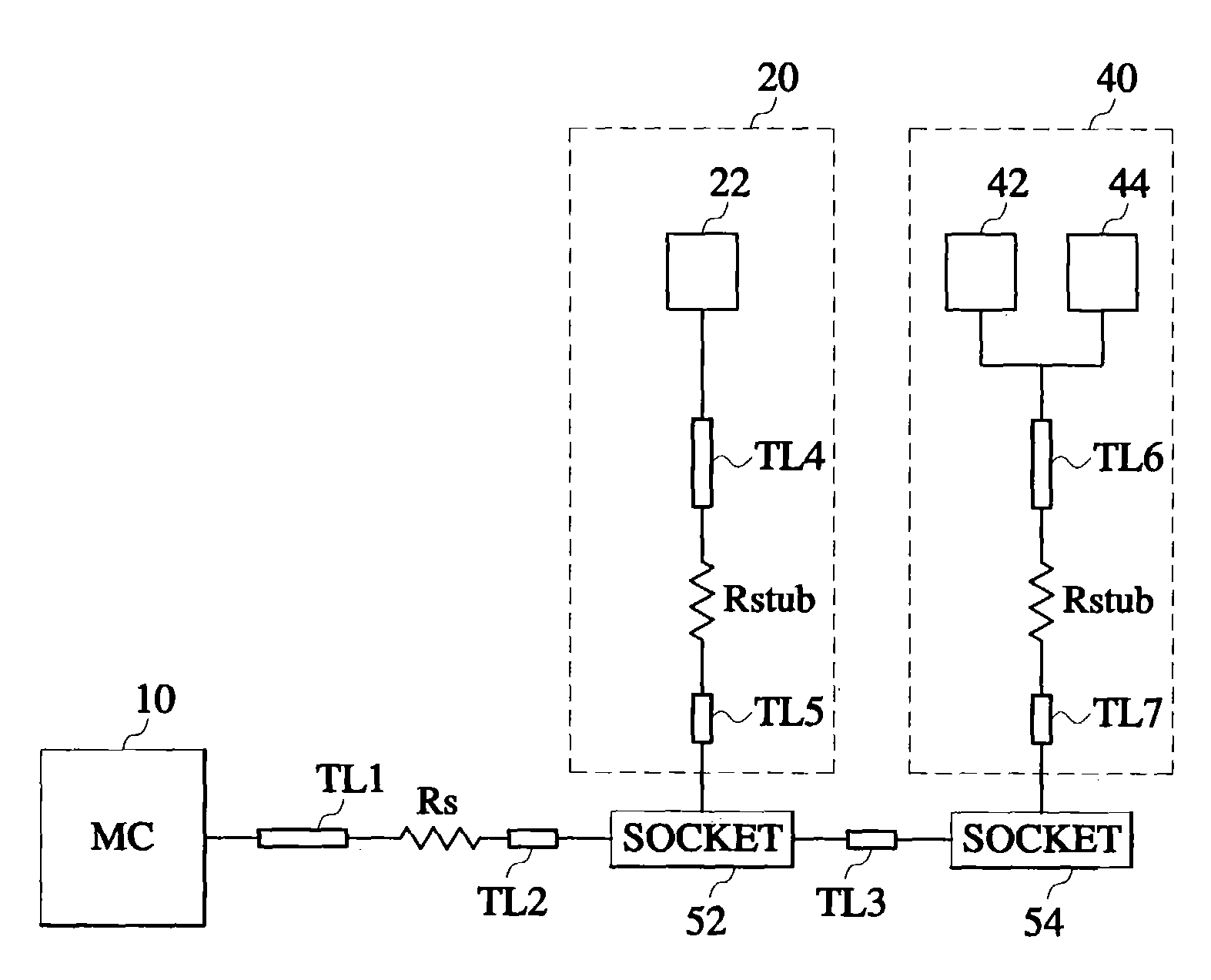
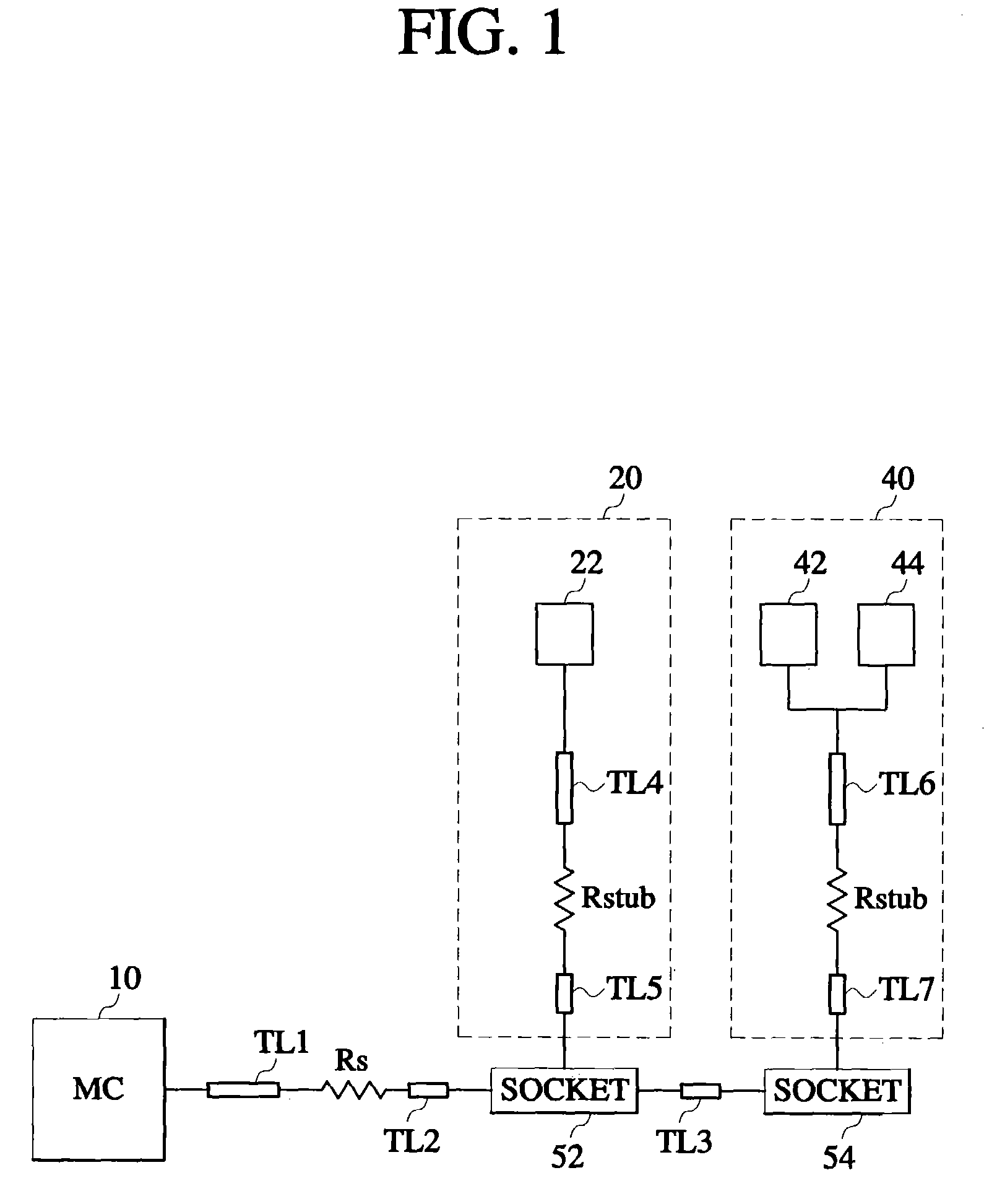
[0017]FIG. 1 illustrates a block diagram of a memory system in accordance with the present invention. As shown in FIG. 1, the memory system includes one single in-line memory module (SIMM) 20 and one dual in-line memory module (DIMM) 40. In fact, a memory system may include more than one SIMM and DIMM. There may be other semiconductor devices in the memory system, but only devices connected to a DQ channel are illustrated in FIG. 1.

[0018]In addition to the SIMM 20 and the DIMM 40, the memory system of FIG. 1 includes a memory controller (MC) 10, a first socket 52 for receiving the SIMM 20, a second socket 54 for receiving the DIMM 40, signal transmission lines TL1 and TL2 for transmitting data between the memory controller 10 and the first socket 52, an impedance matching resistive element Rs connected between the memory controller 10 and the first socket 52, and a signal transmission line TL3 for transmitting data between the first socket 52 and the second socket 54.

[0019]SIMM 20 c...


PUM


Abstract

A memory system system includes a single in-line memory module (SIMM) which contains a memory device and a signal transmission line connected between the memory device and a connection terminal, and a dual in-line memory module (DIMM) which contains two memory devices and a signal transmission line connected between the two memory devices and a connection terminal. A length of the signal transmission line of the SIMM is longer than a length of the signal transmission line of the DIMM. The load of the memory device of the SIMM is less than the load of memory devices of the DIMM, and the longer length of the signal transmission line of the SIMM increases a signal delay time of the SIMM to compensate for the different loads of the SIMM and DIMM memory devices. The longer length of the signal transmission line of the SIMM may further compensate for a signal transmission line connected between the first and second sockets which receive the SIMM and DIMM, respectively.

Description

BACKGROUND OF THE INVENTION[0001]1. Field of the Invention[0002]The present invention relates to a memory system, and more particularly, the present invention relates to improving the signal integrity of a memory bus channel of a memory system having different types of memory modules, for example, a dual in-line memory module (DIMM) and a single in-line memory module (SIMM).[0003]A claim of priority is made to Korean Patent Application No. 2002-45914, filed Aug. 2, 2002 and entitled “Memory System”, which is incorporated by reference herein in its entirety.[0004]2. Description of the Related Art[0005]A computer memory system is generally made up of a memory controller chip set, memory devices, resistive elements, and wires mounted on a computer main board. The wires electrically interconnect the memory controller chip set, the memory devices and the resistive elements, and a memory bus channel functions as a data or signal transmission line between the memory controller chip set and...

Claims


Application Information

Patent Timeline
IPC IPC(8): G06F12/00G06F13/40G06F13/12
CPCG06F13/4086G06F13/12
Inventor LEE, JAE-JUNSO, BYUNG-SEPARK, MYUN-JOO
Owner SAMSUNG ELECTRONICS CO LTD
Why Eureka
Try Eureka