

Method for forming a metal oxide film
a metal oxide film and film technology, applied in the direction of coatings, transistors, chemical vapor deposition coatings, etc., can solve the problems of inability to significantly increase the capacitance of capacitors, the thickness of capacitor insulation films becomes less uniform, etc., to achieve excellent step coverage and film qualities, and the effect of increasing the throughput of a semiconductor devi
- Summary
- Abstract
- Description
- Claims
- Application Information
AI Technical Summary
Benefits of technology
Problems solved by technology
Method used
Image

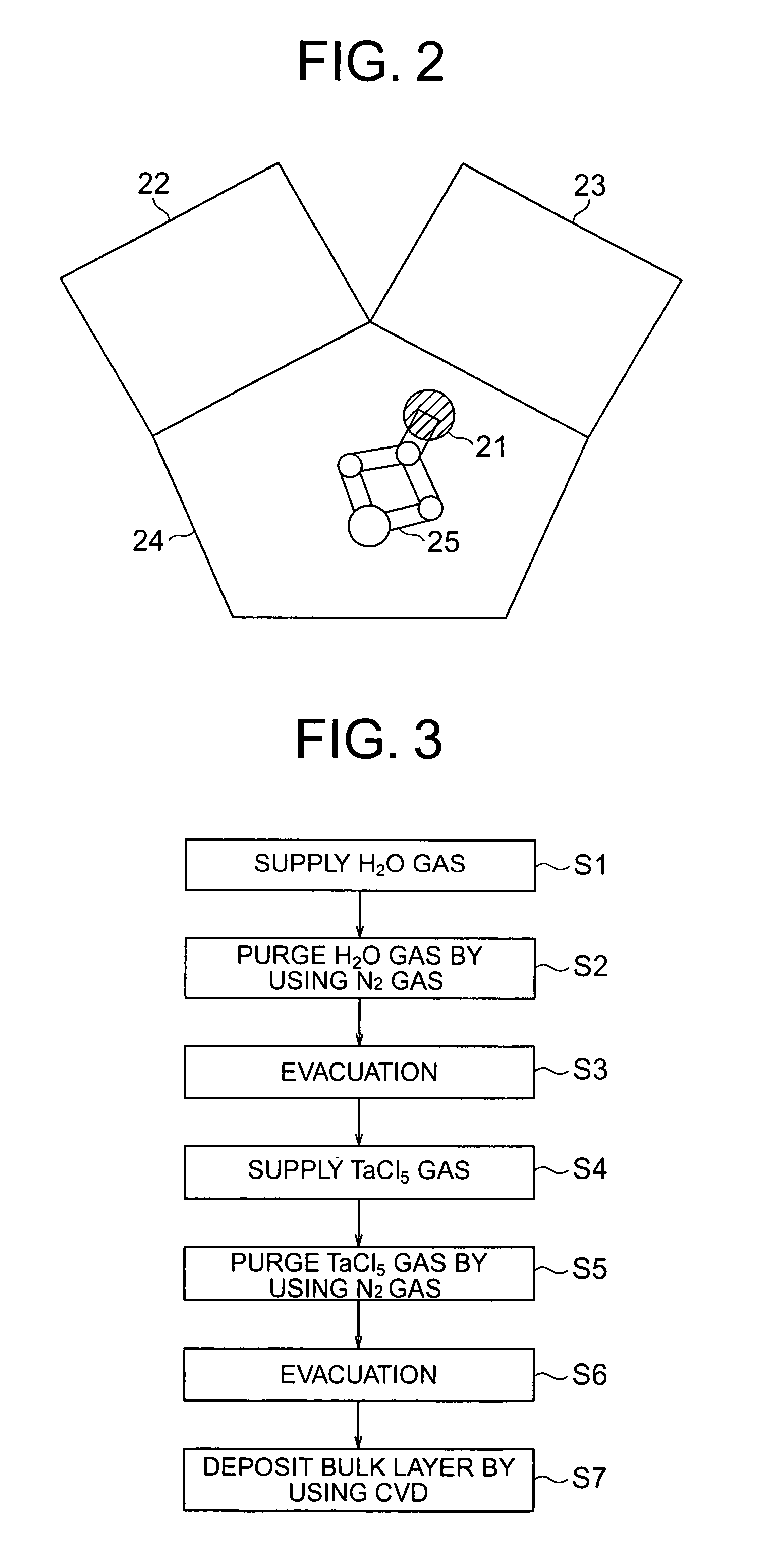
Examples
first embodiment
[First Embodiment]
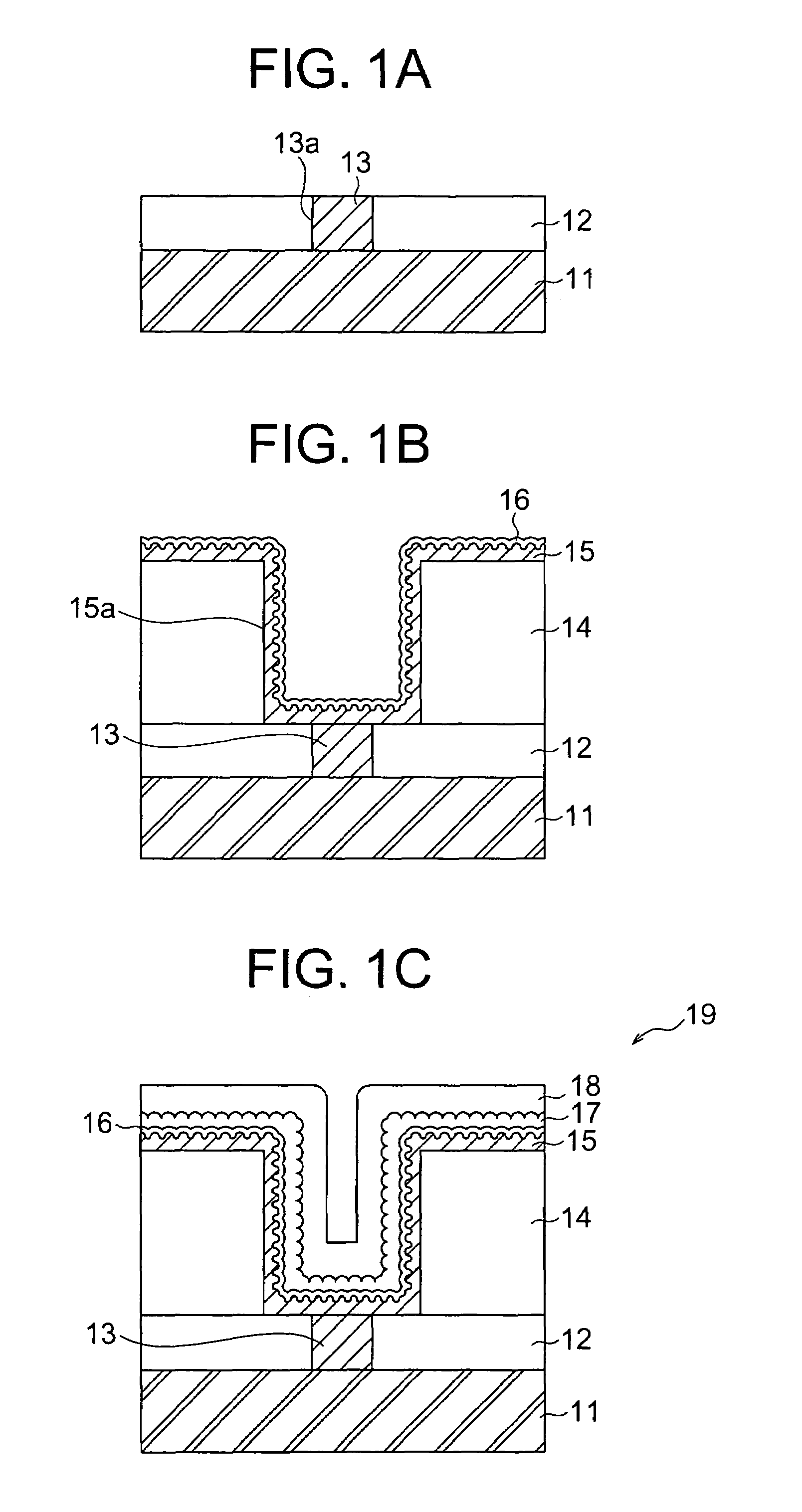
[0029]The present embodiment is an example in which the present invention is applied to a method for forming a capacitor insulation film made of tantalum oxide film. Referring to FIGS. 1A through 1C, there are shown consecutive steps of the process for fabricating the capacitor insulation film according to the present embodiment. Before forming the capacitor insulation film, an underlying film is formed on which the capacitor insulation film is to be deposited. As shown in FIG. 1A, a first interlayer insulating film 12 made of silicon oxide is formed on a silicon substrate 11. Subsequently, a through-hole 13a is formed in the first interlayer insulating film 12 to expose therein a portion of the silicon substrate 11. Thereafter, the through-hole 13a is filled with p-doped polysilicon to form a contact plug 13.
[0030]Then, as shown in FIG. 1B, a second interlayer insulating film 14 made of silicon oxide is formed on the first interlayer insulating film 12 and the con...
second embodiment
[Second Embodiment]
[0042]The present embodiment is an example in which the present invention is again applied to the formation of a capacitor insulation film made of tantalum oxide film. The present embodiment is similar to the first embodiment described above, except that step S1 of the first embodiment is performed in the ambience of active oxygen gas supplied instead of the H2O gas in the reaction chamber.
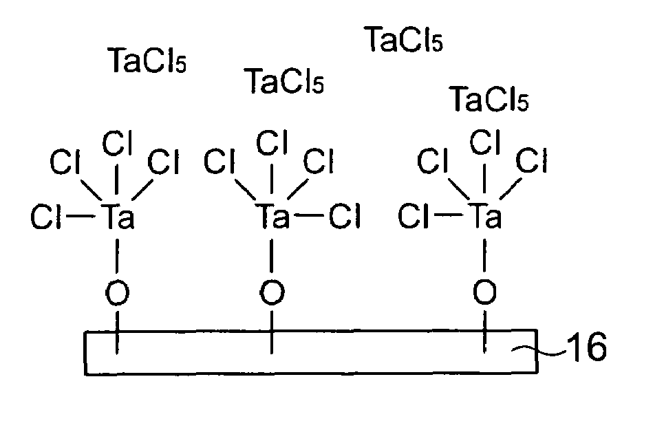
[0043]In the present embodiment, the supply of the active oxygen gas in step S1 causes oxygen to bind to the surface of the silicon nitride film 16 through oxidation. Then, the provision of the TaCl5 gas in step S4 causes the oxygen, that is bound to the surface of the silicon nitride film 16, to bind with the TaCl4 group in the TaCl5 gas, thereby forming a seed monoatomic layer made of TaCl4 group bound to the O atoms on the surface of the silicon nitride film 16. Therefore, in the present embodiment, as in the first embodiment, the bulk layer made of the tantalum oxide film is...
third embodiment
[Third Embodiment]
[0044]The present embodiment is an example in which the present invention is again applied to the formation of a capacitor insulation film made of tantalum oxide film. FIG. 6 shows the procedures of the present embodiment. The present embodiment is similar to the first embodiment except that step S1′–step S3′ similar to step S1–step S3 in the first embodiment are iterated in the present embodiment.
[0045]More specifically, in step S1′ of the present embodiment, H2O gas is supplied after step S6 under the conditions similar to step S1. As a result, the Cl atoms in the TaCl4 group are replaced with OH atoms (step S1′). Then, N2 gas is supplied under the conditions similar to step S2 so as to purge the remaining H2O gas and the Cl atoms (or HCl gas), that were replaced at step S1′, from the first reaction chamber 22 (step S2′). Then, the chamber is evacuated to vacuum under the conditions similar to step S3 (step S3′).
[0046]In accordance with the present embodiment, st...
PUM
| Property | Measurement | Unit |
|---|---|---|
| dielectric constant | aaaaa | aaaaa |
| dielectric constant | aaaaa | aaaaa |
| temperature | aaaaa | aaaaa |
Abstract
Description
Claims
Application Information