One time programmable memory cell

a memory cell and programmable technology, applied in the direction of solid-state devices, instruments, semiconductor/solid-state device details, etc., can solve the problem of degrading the breakdown property of thin oxide, and achieve the effect of avoiding inter-poly oxide low breakdown, convenient generation and convenient induction

Active Publication Date: 2007-08-14
ALPHA & OMEGA SEMICON LTD
View PDF1 Cites 35 Cited by
  • Summary
  • Abstract
  • Description
  • Claims
  • Application Information

AI Technical Summary

Benefits of technology

[0008]Specifically, it is an object of the present invention to provide a one-time programmable (OTP) memory cell by taking advantage of the sidewall and corner breakdown features of a thin oxide layer overlying a polysilicon segment. The phenomena of etch undercut prior to the gate oxidation further degrades the breakdown property of the thin oxide. In general, special attention needs to be paid to avoid the inter-poly oxide low breakdown issues in conventional IC poly-poly capacitors or flash / EEPROM memory interpoly coupling layers (for example, high quality oxide-nitride-oxide composite layers are commonly used). However in this invention disclosure, the weakness of the inter-poly sidewall oxide breakdown is utilized to our advantage as a programming mechanism for the OTP cell. As a breakdown and conductivity between two polysilicon layers can be more conveniently generated, this undesirable poly segment sidewall configuration is implemented for inducing a breakdown and for changing the conductivity state to perform the one-time program function.
[0009]Briefly in a preferred embodiment this invention discloses a one-time programmable (OTP) memory cell. The OTP memory cell includes a dielectric layer disposed between two conductive polysilicon segments wherein the dielectric layer is ready to change from a non-conductive state to a conductive state through an induced voltage breakdown. In a preferred embodiment, one of the conductive polysilicon segments further includes an etch undercut configuration for conveniently inducing the voltage breakdown in the dielectric layer. In another preferred embodiment, one of the conductive polysilicon segments further includes an etch undercut configuration for conveniently inducing the voltage breakdown in the dielectric layer via a corner electrical field effect. In another preferred embodiment, the dielectric layer constituting a sidewall covering one of the conductive polysilicon segments with an etch undercut configuration for inducing the voltage breakdown in the dielectric layer via an edge electrical field effect. In another preferred embodiment, one of the conductive polysilicon segments further includes a corner for conveniently inducing the voltage breakdown in the dielectric layer via a corner electrical field effect. In another preferred embodiment, the OTP memory cell further includes a semiconductor substrate having an insulating layer disposed on a top surface of the substrate for supporting the OTP memory cell thereon. In another preferred embodiment, the OTP memory cell further includes an insulating passivation layer covering the OTP memory cell and the insulating passivation layer further includes contact opening for depositing electrode metal therein to for electrically contacting the conductive polysilicon segments to function as electrodes. In another preferred embodiment, the conductive polysilicon segments are conductive impurity doped polysilicon segments. The conductive polysilicon segments can be a P-type impurity doped or N-type impurity doped polysilicon segment.
[0010]This invention further discloses a method for manufacturing a one-time programmable (OTP) memory cell. The method includes a step of disposing a dielectric layer between two conductive polysilicon segments for readily inducing a voltage breakdown in the dielectric to change from a non-conductive state to a conductive state for carrying out a one-time program operation. In another preferred embodiment, the method further includes a step of forming one of the conductive polysilicon segments with an etch undercut configuration for conveniently inducing the voltage breakdown in the dielectric layer. In another preferred embodiment, the method further includes a step of forming one of the conductive polysilicon segments with an etch undercut configuration with a corner for conveniently inducing the voltage breakdown in the dielectric layer via a corner electrical field effect. In another preferred embodiment, the method further includes a step of forming one of the dielectric layer as a sidewall covering one of the conductive polysilicon segments with an etch undercut configuration for inducing the voltage breakdown in the dielectric layer via an edge electrical field effect. In another preferred embodiment, the method further includes a step of forming one of the conductive polysilicon segments with a corner for conveniently inducing the voltage breakdown in the dielectric layer via a corner electrical field effect.

Problems solved by technology

The phenomena of etch undercut prior to the gate oxidation further degrades the breakdown property of the thin oxide.

Method used


Image

  • One time programmable memory cell
  • One time programmable memory cell
  • One time programmable memory cell

Examples


Embodiment Construction

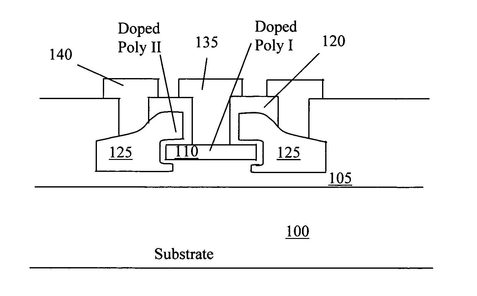
[0014]Referring to FIG. 1 for a one-time programmable memory cell of this invention supported on a thick field oxide layer 100 formed on a top surface of a semiconductor substrate 100. The thick field oxide layer 105 insulates the cell from the substrate 100. A first doped poly region 210 is insulted with a thin layer low voltage gate oxide 120 from a second doped polysilicon region 125. Each poly region has an electrode, e.g., electrodes 135 and 140 respectively, connected for data recording and reading. The thin gate oxide layer 120 between the two doped poly regions blocks the conductivity between the two doped poly regions 110 and 125. However, the conducting status between the two doped poly regions 110 and 125 may be changed for the purpose of programming the memory. In the process of programming the memory cell as shown in FIG. 1, a high voltage may be applied to the electrodes between doped poly regions 110 and 125. When the voltage is high enough, a breakdown is induced in ...


PUM


Abstract

This invention discloses a one-time programmable (OTP) memory cell. The OTP memory cell includes a dielectric layer disposed between two conductive polysilicon segments wherein the dielectric layer is ready to change from a non-conductive state to a conductive state through an induced voltage breakdown. In a preferred embodiment, one of the conductive polysilicon segments further includes an etch undercut configuration for conveniently inducing the voltage breakdown in the dielectric layer. In a preferred embodiment, the dielectric layer is further formed as sidewalls covering the edges and corners of a first polysilicon segments to conveniently induce a voltage breakdown in the dielectric layer by the edge and corner electrical field effects.

Description

BACKGROUND OF THE INVENTION[0001]1. Field of the Invention[0002]The invention disclosed herein relates generally to the structure and manufacturing process of a memory cell. More particularly, this invention relates to a novel cell structure and manufacturing process of a write once programmable memory.[0003]2. Description of the Prior Art[0004]In order to reduce cost and to shorten the time-to-market of integrated circuit (IC) products, the design houses are increasingly relying on the readily available foundry processes to carry out the prototyping and manufacturing. However, the device features that are tailored for post-package trimming require additional intellectual property (IP) modules or fuse. These IP modules may include one time programmable (OTP) memory or the electrical erasable programmable read only memory (EEPROM) provided by the foundry with additional costs. In the case of fuse, fuse-trimming using dedicated testing equipment with specific test configuration setup ...

Claims


Application Information

Patent Timeline
Patent Type & Authority Patents(United States)
IPC IPC(8): H01L29/788
CPCG11C17/16G11C17/18H01L27/112H01L27/11206H10B20/00H10B20/20
Inventor HU, YONGZHONGTAI, SUNG-SHAN
Owner ALPHA & OMEGA SEMICON LTD
Why Eureka
Try Eureka