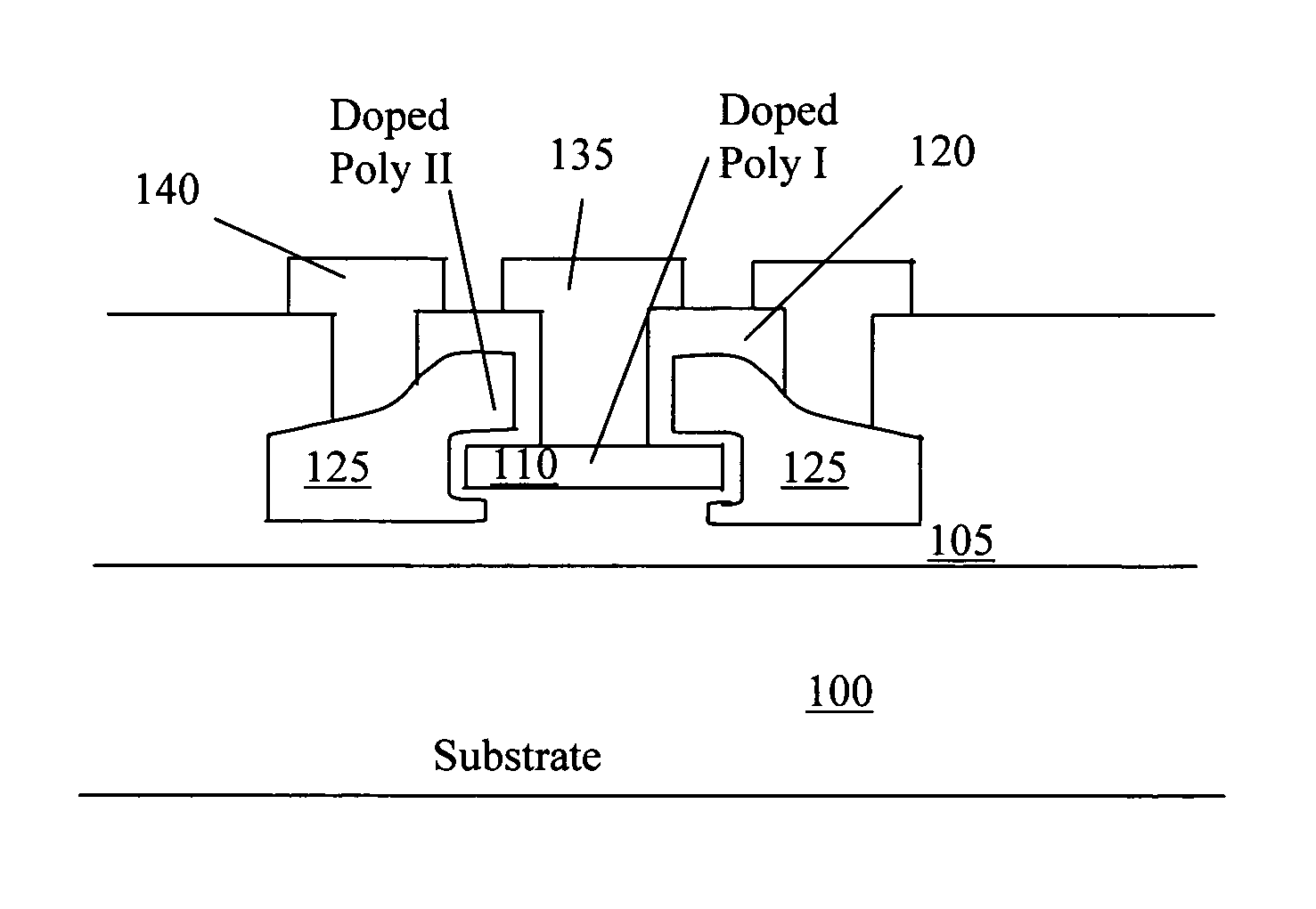
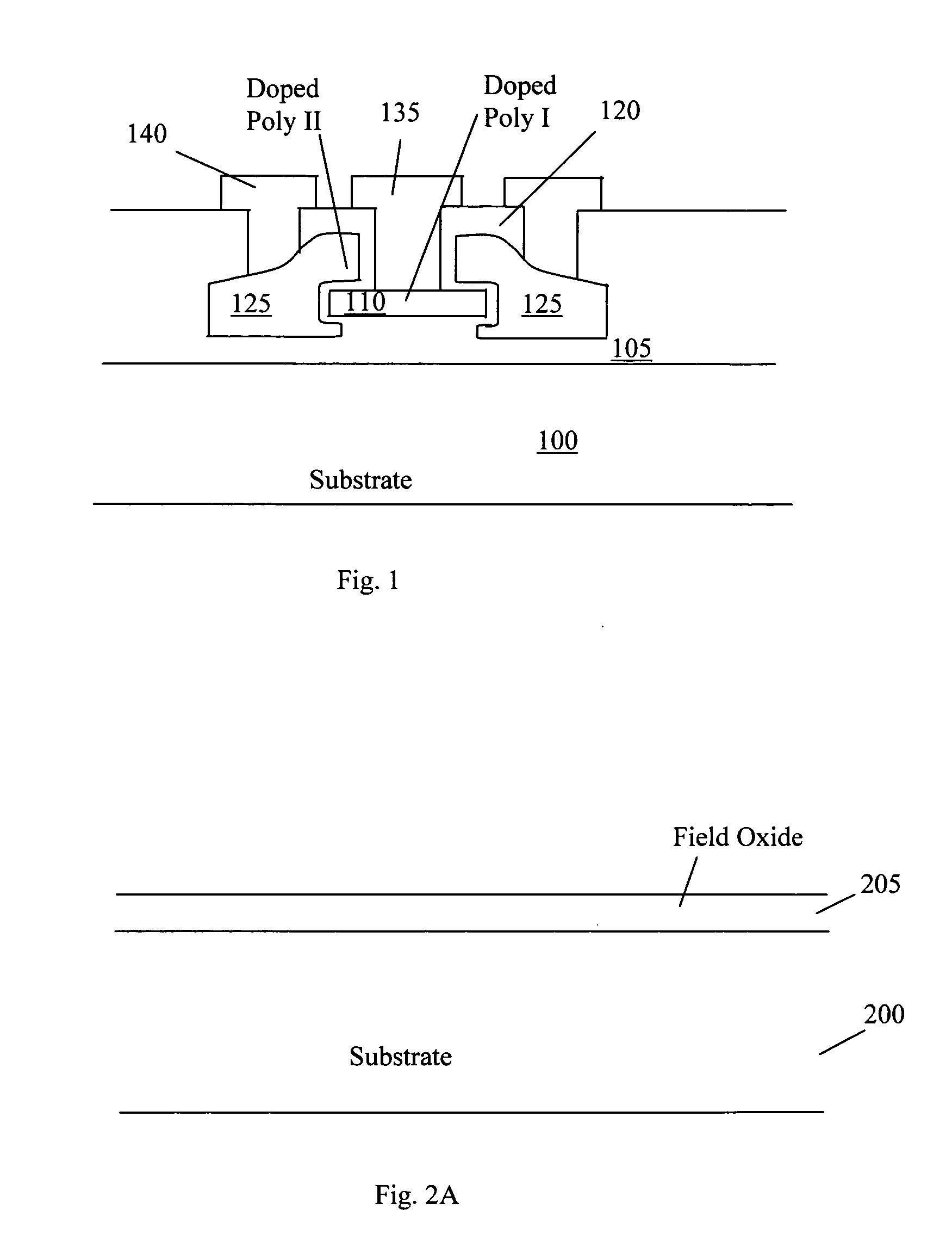
[0008] Specifically, it is an object of the present invention to provide a one-time programmable (OTP) memory
cell by taking
advantage of the sidewall and corner breakdown features of a
thin oxide layer overlying a polysilicon segment. The phenomena of etch
undercut prior to the gate oxidation further degrades the breakdown property of the
thin oxide. In general, special attention needs to be paid to avoid the inter-poly
oxide low breakdown issues in conventional IC poly-poly capacitors or flash /
EEPROM memory interpoly
coupling layers (for example, high quality
oxide-
nitride-
oxide composite
layers are commonly used). However in this invention disclosure, the
weakness of the inter-poly sidewall oxide breakdown is utilized to our
advantage as a
programming mechanism for the OTP
cell. As a breakdown and
conductivity between two polysilicon
layers can be more conveniently generated, this undesirable poly segment sidewall configuration is implemented for inducing a breakdown and for changing the
conductivity state to perform the one-time program function.
[0009] Briefly in a preferred embodiment this invention discloses a one-time programmable (OTP) memory cell. The OTP memory cell includes a
dielectric layer disposed between two conductive polysilicon segments wherein the dielectric layer is ready to change from a non-conductive state to a conductive state through an
induced voltage breakdown. In a preferred embodiment, one of the conductive polysilicon segments further includes an etch undercut configuration for conveniently inducing the
voltage breakdown in the dielectric layer. In another preferred embodiment, one of the conductive polysilicon segments further includes an etch undercut configuration for conveniently inducing the voltage breakdown in the dielectric layer via a corner electrical
field effect. In another preferred embodiment, the dielectric layer constituting a sidewall covering one of the conductive polysilicon segments with an etch undercut configuration for inducing the voltage breakdown in the dielectric layer via an edge electrical
field effect. In another preferred embodiment, one of the conductive polysilicon segments further includes a corner for conveniently inducing the voltage breakdown in the dielectric layer via a corner electrical
field effect. In another preferred embodiment, the OTP memory cell further includes a
semiconductor substrate having an insulating layer disposed on a top surface of the substrate for supporting the OTP memory cell thereon. In another preferred embodiment, the OTP memory cell further includes an insulating
passivation layer covering the OTP memory cell and the insulating
passivation layer further includes contact opening for depositing
electrode metal therein to for electrically contacting the conductive polysilicon segments to function as electrodes. In another preferred embodiment, the conductive polysilicon segments are conductive
impurity doped polysilicon segments. The conductive polysilicon segments can be a P-type
impurity doped or N-type
impurity doped polysilicon segment.
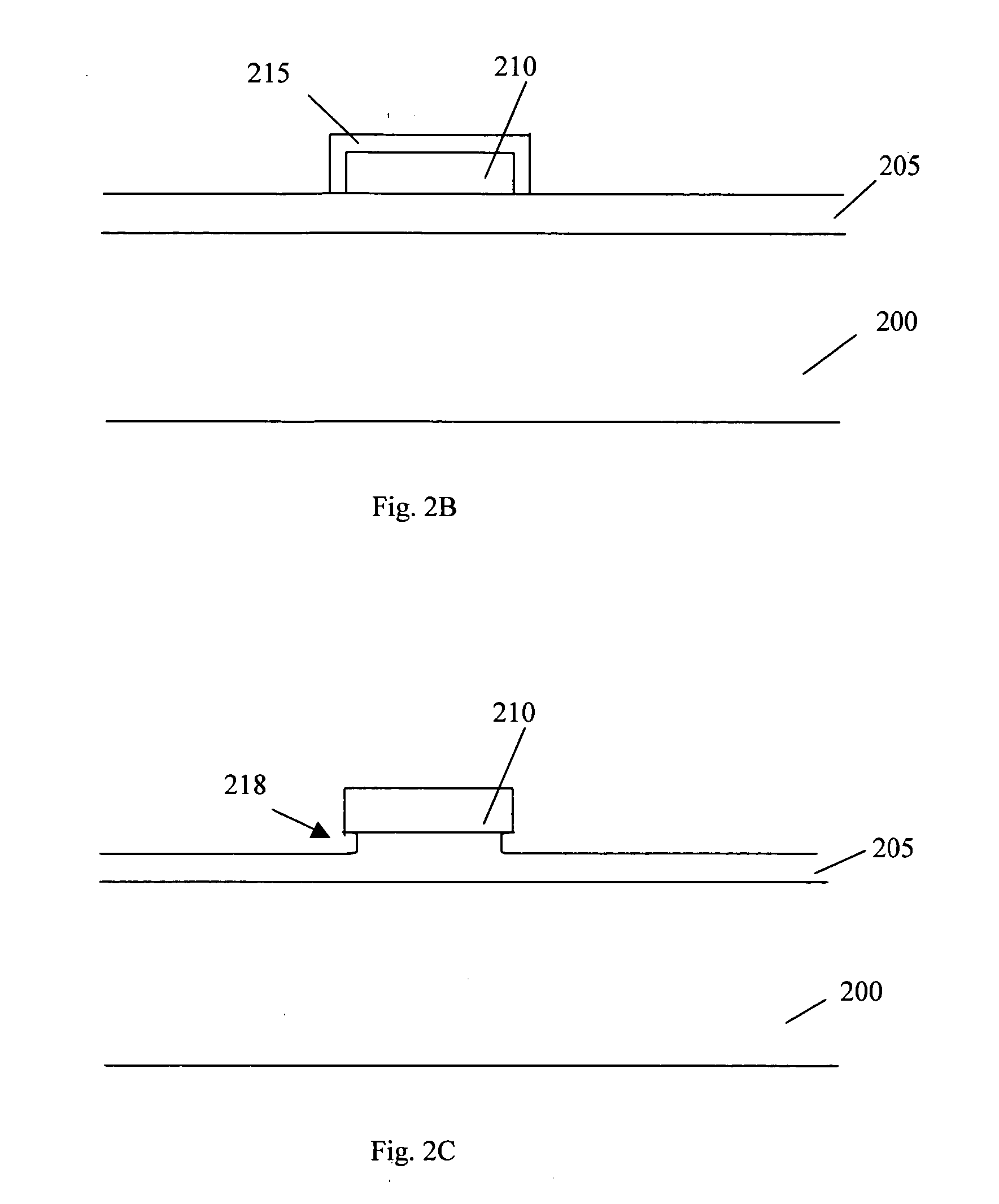
[0010] This invention further discloses a method for manufacturing a one-time programmable (OTP) memory cell. The method includes a step of disposing a dielectric layer between two conductive polysilicon segments for readily inducing a voltage breakdown in the dielectric to change from a non-conductive state to a conductive state for carrying out a one-time program operation. In another preferred embodiment, the method further includes a step of forming one of the conductive polysilicon segments with an etch undercut configuration for conveniently inducing the voltage breakdown in the dielectric layer. In another preferred embodiment, the method further includes a step of forming one of the conductive polysilicon segments with an etch undercut configuration with a corner for conveniently inducing the voltage breakdown in the dielectric layer via a corner electrical field effect. In another preferred embodiment, the method further includes a step of forming one of the dielectric layer as a sidewall covering one of the conductive polysilicon segments with an etch undercut configuration for inducing the voltage breakdown in the dielectric layer via an edge electrical field effect. In another preferred embodiment, the method further includes a step of forming one of the conductive polysilicon segments with a corner for conveniently inducing the voltage breakdown in the dielectric layer via a corner electrical field effect.

