Semiconductor waveguide based high speed all optical wavelength converter

a technology of semiconductors and wavelength converters, applied in non-linear optics, instruments, light demodulation, etc., can solve the problems of high cost, photorefractive damage, and known wavelength conversion techniques such as those used in linbosub>3/sub>crystal based wavelength converters,

Inactive Publication Date: 2007-08-14
INTEL CORP
View PDF2 Cites 22 Cited by
  • Summary
  • Abstract
  • Description
  • Claims
  • Application Information

AI Technical Summary

Problems solved by technology

Known wavelength conversion techniques such as for example those that have been used in LiNbO3 crystal based wavelength converters have suffered from issues such as photorefractive damage and high cost.

Method used


Image

  • Semiconductor waveguide based high speed all optical wavelength converter
  • Semiconductor waveguide based high speed all optical wavelength converter
  • Semiconductor waveguide based high speed all optical wavelength converter

Examples


Embodiment Construction

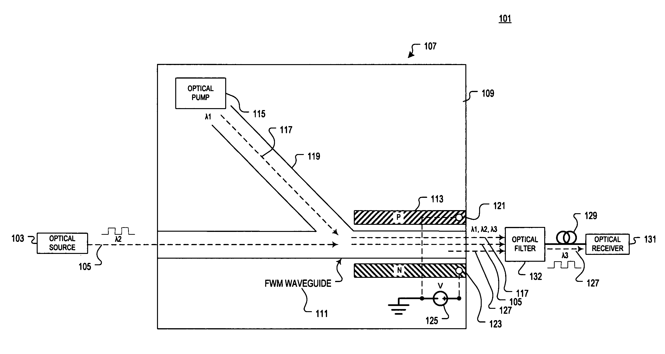
[0013]Methods and apparatuses for converting a wavelength of an optical beam are disclosed. In the following description numerous specific details are set forth in order to provide a thorough understanding of the present invention. It will be apparent, however, to one having ordinary skill in the art that the specific detail need not be employed to practice the present invention. In other instances, well-known materials or methods have not been described in detail in order to avoid obscuring the present invention.

[0014]Reference throughout this specification to “one embodiment” or “an embodiment” means that a particular feature, structure or characteristic described in connection with the embodiment is included in at least one embodiment of the present invention. Thus, appearances of the phrases “in one embodiment” or “in an embodiment” in various places throughout this specification are not necessarily all referring to the same embodiment. Furthermore, the particular features, stru...


PUM

PropertyMeasurementUnit
wavelengthaaaaaaaaaa

Abstract

A semiconductor-based all optical wavelength converter is disclosed. An apparatus according to aspects of the present invention includes an optical waveguide disposed in semiconductor material. An optical pump source is optically coupled to direct an optical pump beam having a first wavelength into the optical waveguide. The optical waveguide is further optically coupled to receive an input optical beam having a second wavelength. The optical waveguide is optically coupled to generate an output optical beam having a third wavelength in response to the optical pump beam and the input optical beam in the optical waveguide. A diode structure is disposed in the optical waveguide. The diode structure includes at least P and N regions. The diode structure is biased to generate an electric field to remove free carriers from an optical path through the optical waveguide generated in response to two photon absorption in the optical waveguide.

Description

BACKGROUND OF THE INVENTION[0001]1. Field of the Invention[0002]Embodiments of invention relate generally to optical devices and, more specifically but not exclusively relate to semiconductor-based optical wavelength conversion.[0003]2. Background Information[0004]The need for fast and efficient optical-based technologies is increasing as Internet data traffic growth rate is overtaking voice traffic pushing the need for fiber optical communications. Transmission of multiple optical channels over the same fiber in the dense wavelength-division multiplexing (DWDM) system provides a simple way to use the unprecedented capacity (signal bandwidth) offered by fiber optics. Commonly used optical components in the system include wavelength division multiplexed (WDM) transmitters and receivers, optical filter such as diffraction gratings, thin-film filters, fiber Bragg gratings, arrayed-waveguide gratings, optical add / drop multiplexers and wavelength converters.[0005]A wavelength converter i...

Claims


Application Information

Patent Timeline
Patent Type & Authority Patents(United States)
IPC IPC(8): G02F2/02G02F1/365
CPCG02F1/025G02F1/353G02F1/3536G02F2201/063G02F2202/105
Inventor RONG, HAISHENGPANICCIA, MARIO J.
Owner INTEL CORP
Why Eureka
Try Eureka