

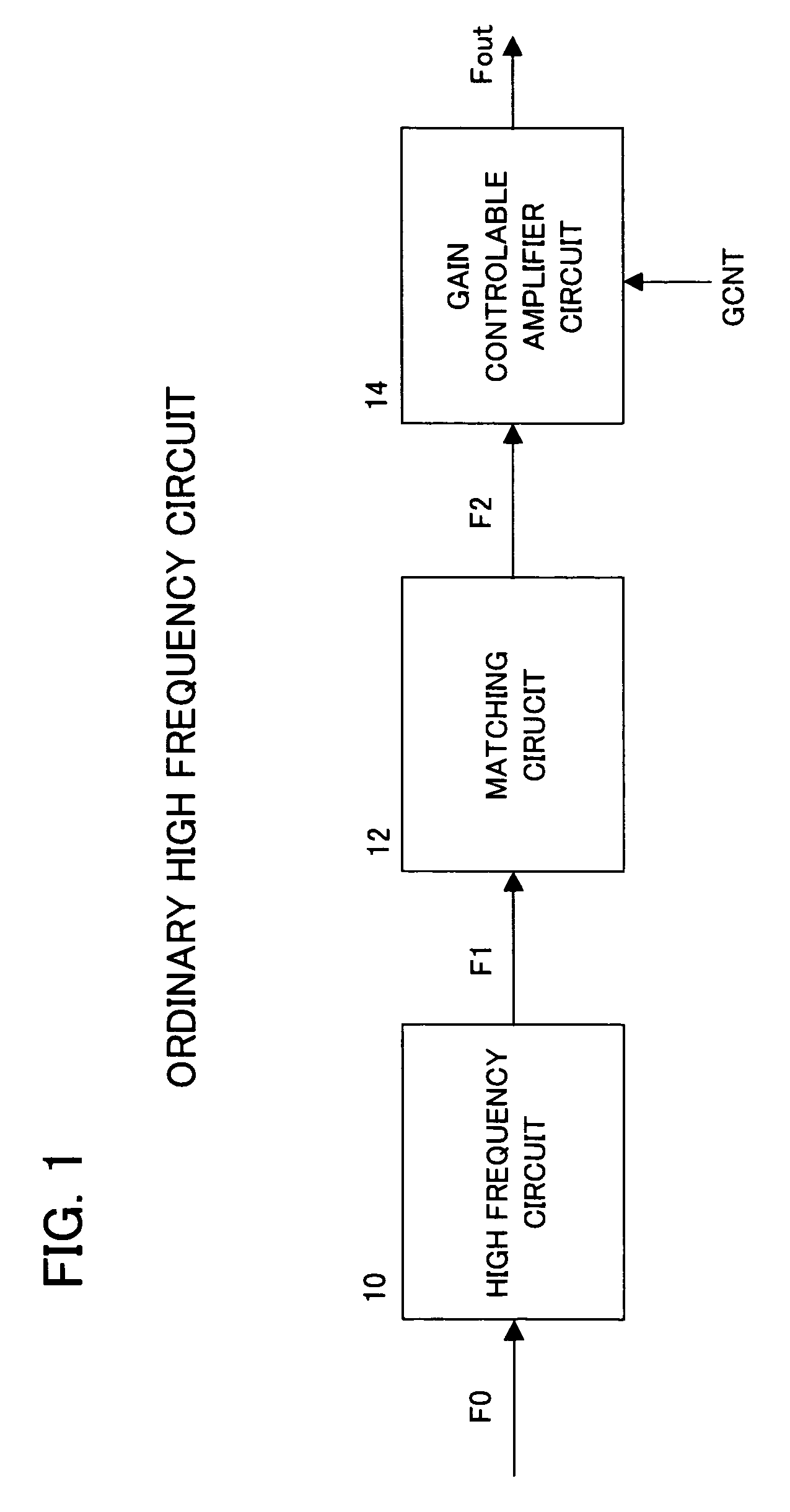
High frequency amplifier circuit permitting variable gain control
a variable gain control and amplifier technology, applied in amplifier modifications to reduce non-linear distortion, power management, wireless communication, etc., can solve the problem of deterioration of the high frequency characteristic, negative effect on the linearity of the attenuator, and the noise figure (nf), which is the ratio between the input sn ratio and the output sn ratio
- Summary
- Abstract
- Description
- Claims
- Application Information
AI Technical Summary
Benefits of technology
Problems solved by technology
Method used
Image

Examples
Embodiment Construction
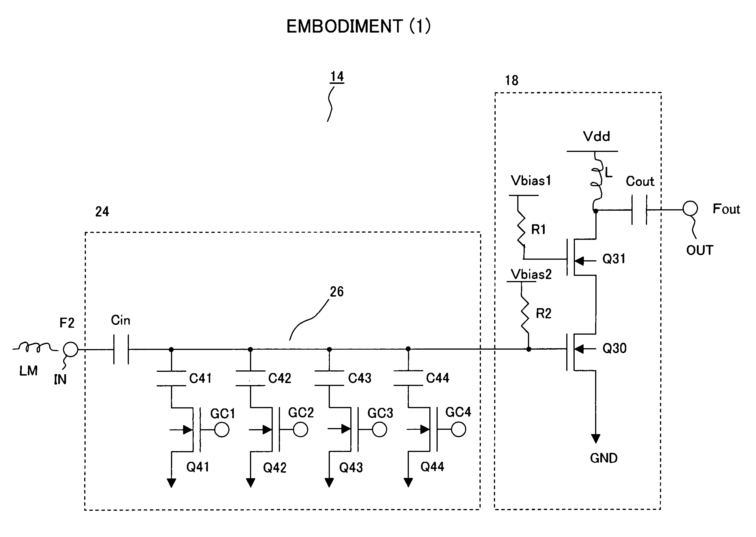
[0023]An embodiment of the present invention will be described hereinbelow with reference to the drawings. However, the technical scope of the present invention is not limited to or by this embodiment and is intended to cover the items appearing in the claims as well as any equivalents thereof.
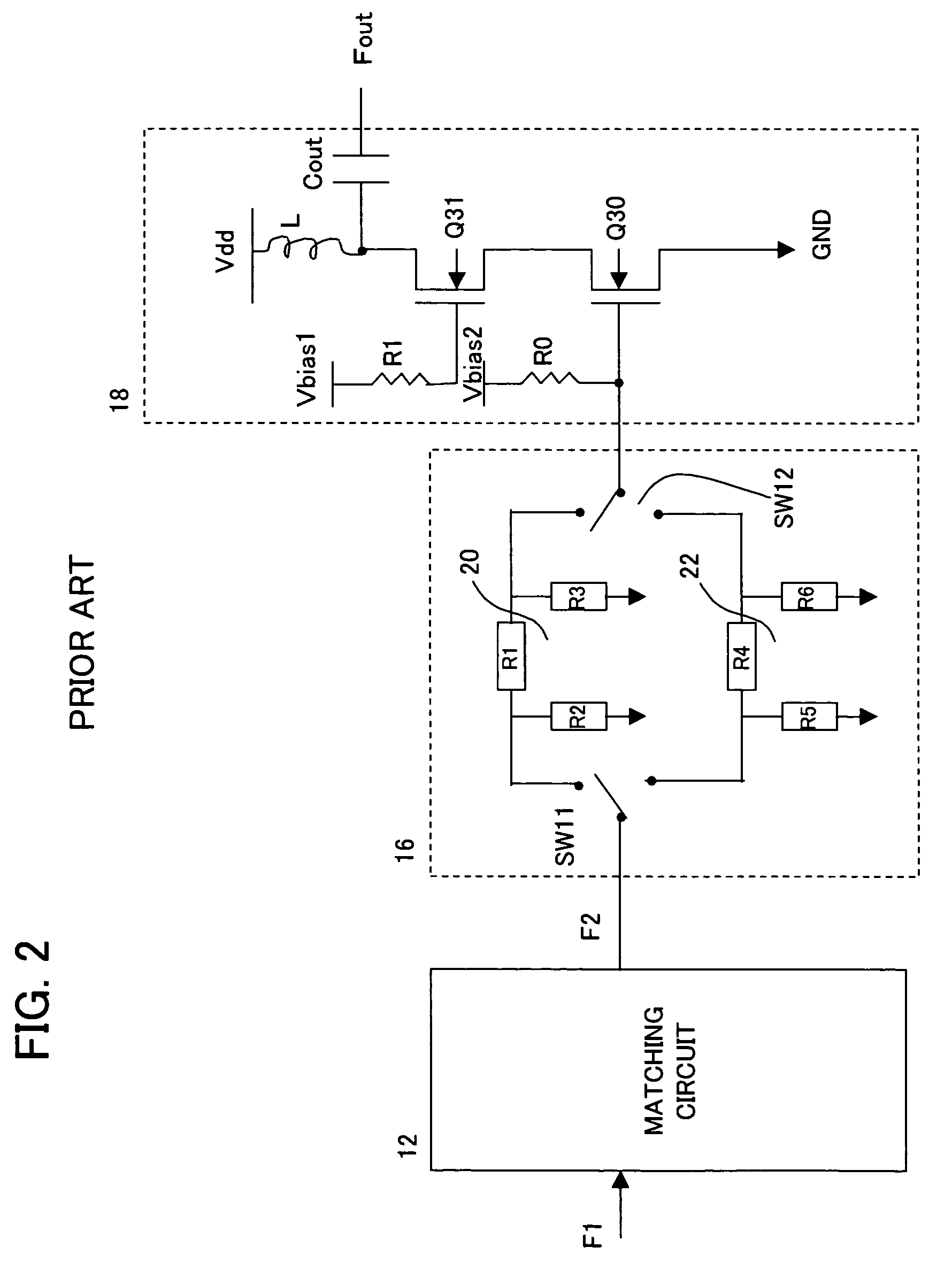
[0024]FIG. 3 is a circuit diagram of the amplifier circuit of this embodiment. In this amplifier circuit, a variable attenuator 24 is provided upstream of an amplifier transistor unit 18. The constitution of the amplifier transistor unit 18 is the same as the example in FIG. 2 and therefore the same reference numbers have been assigned. This amplifier circuit is constituted by MOS transistors Q30, Q31, capacitive element Cout, resistive element R1, R2, and inductance element L, and so forth, which are provided on a silicon substrate.
[0025]The amplifier transistor unit 18 is provided with an N-channel transistor Q30 whose gate is supplied with the high frequency input signal F2 from the input t...
PUM
 Abstract
Description
Claims
Application Information