Low energy dose monitoring of implanter using implanted wafers

a low energy dose and implanter technology, applied in the field of integrated circuits, can solve problems such as the crystallization of amorphous silicon materials, and achieve the effects of low energy dose, high device yield per wafer, and convenient us

Active Publication Date: 2007-08-21
SEMICON MFG INT (SHANGHAI) CORP
View PDF8 Cites 2 Cited by
  • Summary
  • Abstract
  • Description
  • Claims
  • Application Information

AI Technical Summary

Benefits of technology

[0012]Many benefits are achieved by way of the present invention over conventional techniques. For example, the present technique provides an easy to use process that relies upon conventional technology. In some embodiments, the method provides higher device yields in dies per wafer. Additionally, the method provides a process that is compatible with conventional process technology without substantial modifications to conventional equipment and processes. Preferably, the invention can be applied to a variety of applications such as memory, ASIC, microprocessor, and other devices. Preferably, the invention provides a way to monitor a low energy dose implantation process for shallow junction devices. Depending upon the embodiment, one or more of these benefits may be achieved. These and other benefits will be described in more throughout the present specification and more particularly below.

Problems solved by technology

Preferably, the amorphous state traps the dopant particles and may even cause recrystallization of the amorphous silicon material.

Method used


Image

  • Low energy dose monitoring of implanter using implanted wafers
  • Low energy dose monitoring of implanter using implanted wafers
  • Low energy dose monitoring of implanter using implanted wafers

Examples


Embodiment Construction

[0017]According to the present invention, techniques for processing for the manufacture of semiconductor devices are provided. But it would be recognized that the invention has a much broader range of applicability. More particularly, the invention provides a method for monitoring a low energy dose implantation process for the manufacture of integrated circuits. For example, the invention can be applied to a variety of devices such as static random access memory devices (SRAM), application specific integrated circuit devices (ASIC), microprocessors and micro controllers, Flash memory devices, and others.

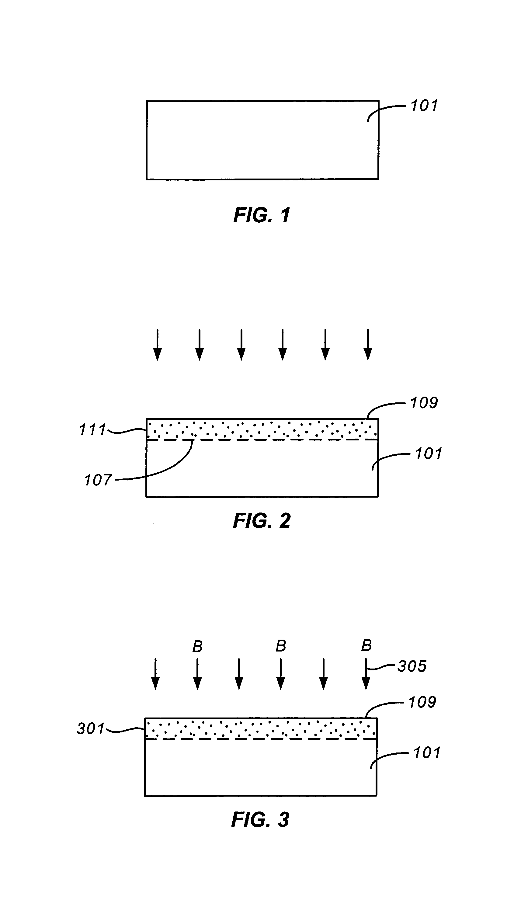
[0018]A method for fabricating a monitor substrate to monitor a low energy dose implantation process according to an embodiment of the present invention is provided as follows:

[0019]1. Provide a monitor wafer, e.g., silicon wafer;

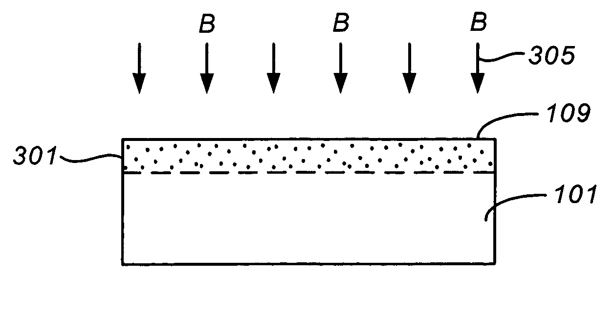
[0020]2. Introduce a plurality of particles (e.g., silicon) within a depth of the silicon material to cause an amorphous state within the silicon material;

[...


PUM

PropertyMeasurementUnit
energyaaaaaaaaaa
energyaaaaaaaaaa
shallow junction depthaaaaaaaaaa

Abstract

A method for processing semiconductor wafers, e.g., silicon. The method includes providing a monitor wafer, which is made of a crystalline material. The method includes introducing a plurality of particles within a depth of the material, whereupon the plurality of particles cause the crystalline material to be in an amorphous state. The method also includes introducing a plurality of dopant particles into a selected depth of the crystalline material in the amorphous state using an implantation tool. The amorphous state traps the dopant particles. The method includes subjecting the monitor wafer including the plurality of particles and dopant particles into thermal anneal process to activate the dopant. The sheet resistivity is measured. The method operates the implantation tool using one or more production wafers if the dose of the dopant particles in the monitor water is within a tolerance of a specification limit.

Description

CROSS-REFERENCES TO RELATED APPLICATIONS[0001]NOT APPLICABLESTATEMENT AS TO RIGHTS TO INVENTIONS MADE UNDER FEDERALLY SPONSORED RESEARCH OR DEVELOPMENT[0002]NOT APPLICABLEREFERENCE TO A “SEQUENCE LISTING,” A TABLE, OR A COMPUTER PROGRAM LISTING APPENDIX SUBMITTED ON A COMPACT DISK.[0003]NOT APPLICABLEBACKGROUND OF THE INVENTION[0004]The present invention is directed integrated circuits and their processing for the manufacture of semiconductor devices. More particularly, the invention provides a method for monitoring a low energy dose implantation process for the manufacture of integrated circuits. But it would be recognized that the invention has a much broader range of applicability. For example, the invention can be applied to a variety of devices such as dynamic random access memory devices, static random access memory devices (SRAM), application specific integrated circuit devices (ASIC), microprocessors and microcontrollers, Flash memory devices, and others.[0005]Integrated cir...

Claims


Application Information

Patent Timeline
Patent Type & Authority Patents(United States)
IPC IPC(8): G01R31/26H01L21/00H01J37/317H01L21/265H01L21/42H01L21/66H01L21/82H01L23/544
CPCH01L22/20H01L21/26506H01L21/26513H01L22/34
Inventor WU, JINGANGSONG, JIANPENGCHANG, MINGGANGHUANG, CHINTE
Owner SEMICON MFG INT (SHANGHAI) CORP
Why Eureka
Try Eureka