Shallow low energy ion implantation into pad oxide for improving threshold voltage stability

a low energy ion and threshold voltage stability technology, applied in the field of forming semiconductor devices, can solve the problems of leakage problems, does not offer a solution for minimizing threshold voltage variation, etc., and achieve the effect of significantly reducing the variation of threshold voltage stability due to pad oxide thickness variation, low energy implantation, and increasing threshold voltage stability

Inactive Publication Date: 2007-08-21
CHARTERED SEMICONDUCTOR MANUFACTURING
View PDF8 Cites 1 Cited by
  • Summary
  • Abstract
  • Description
  • Claims
  • Application Information

AI Technical Summary

Benefits of technology

[0008]Accordingly, the main object of this invention is to describe a method of forming a semiconductor device with improved threshold voltage stability.
[0009]It is yet another object to form a semiconductor device with improved threshold voltage stability using shallow implantation through pad oxide.
[0010]Another objective of the invention is to form a semiconductor device with improved threshold voltage stability using a sacrificial ion implantation layer.
[0011]In accordance with these objectives, a process is described to form a MOSFET device with increased threshold voltage stability. After forming shallow trench isolation regions using pad nitride / pad oxide mask stack and removing the pad nitride by a selective etch, required dopants are implanted into the pad oxide using low energy implantation. Deep well implantation is then followed. Using this procedure of sacrificial shallow implantation into the pad oxide prior to well implantation, threshold voltage stability variation due to pad oxide thickness variation is significantly decreased.

Problems solved by technology

Large divot depths cause leakage problems, particularly for 100 nm node device generation.
The first three prior arts do not address the problem of well ion implantation through the pad oxide; the fourth one does not offer a solution for minimizing the threshold voltage variation resulting from through-pad-oxide implantation.

Method used


Image

  • Shallow low energy ion implantation into pad oxide for improving threshold voltage stability
  • Shallow low energy ion implantation into pad oxide for improving threshold voltage stability
  • Shallow low energy ion implantation into pad oxide for improving threshold voltage stability

Examples


Embodiment Construction

[0021]The objects, advantages, and details of fabricating a semiconductor device according to this invention will be more clearly understood from the following detailed description taken in conjunction with the accompanying drawings.

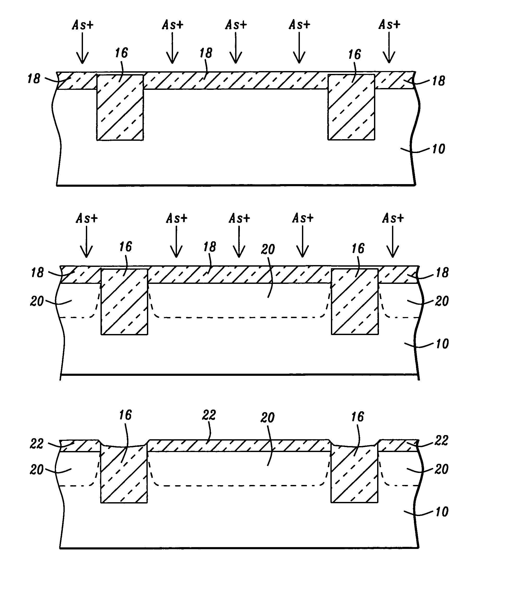
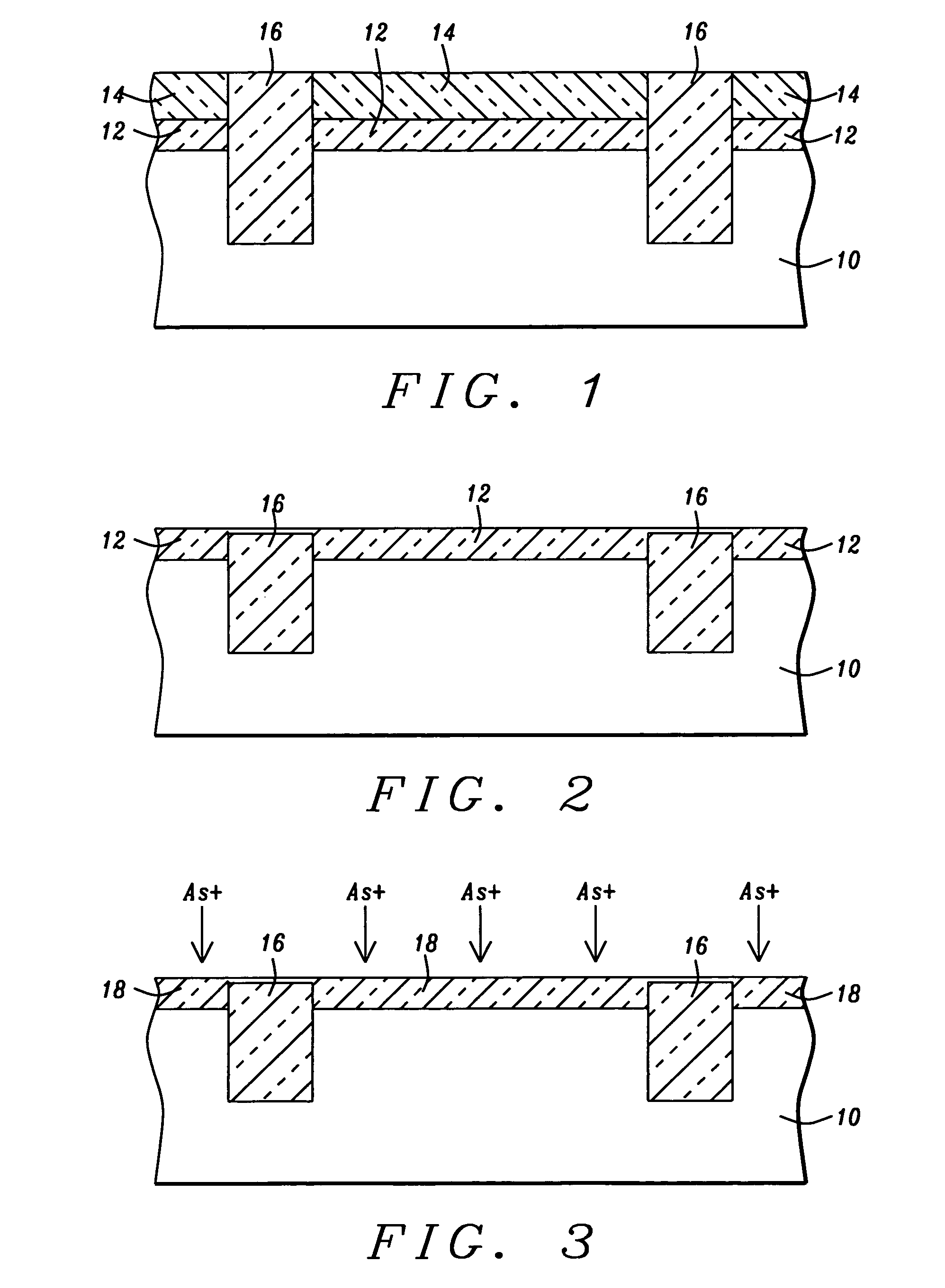
[0022]For the purpose of fabricating a MOSFET device, firstly shallow trench isolation regions are formed as follows: over a semiconductor substrate 10 such as silicon, using chemical vapor deposition (CVD) or plasma-enhanced CVD methods, deposit pad oxide 12 in the range of approximately about 25-120 Å thick and pad nitride 14 in the range of approximately about 500-2000 Å thick; using a plasma process, pattern the pad nitride using a resist mask; using nitride as a mask etch into pad oxide and into the silicon substrate to the desired depth of the shallow trench, in the range of approximately about 2000-5000 Å using suitable plasma processes known in prior art; fill the shallow trenches with a suitable dielectric material 16 such as silicon dioxide; pl...


PUM


Abstract

A method is described to fabricate a MOSFET device with increased threshold voltage stability. After the pad oxide and pad nitride are deposited on the silicon substrate and shallow trenches are patterned and the pad nitride removed. As+ or P+ species are then implanted using low energy ions of approximately 5 keV into the pad oxide. Conventional As+ or P+ implant follows the shallow implant to form the n-wells. With this procedure of forming a sacrificial shallow implantation oxide layer, surface dopant concentration variation at pad oxide:silicon substrate interface is minimized; and threshold voltage stability variation of the device is significantly decreased.

Description

FIELD OF THE INVENTION[0001]The present invention relates generally to a method of forming a semiconductor device, and more particularly to form an MOS transistor with improved threshold voltage stability with the use of a sacrificial ion implantation layer.DESCRIPTION OF THE PRIOR ART[0002]During the fabrication of shallow trench isolation regions in MOSFET devices, the current practice is to sometimes skip depositing a transfer gate sacrificial silicon dioxide layer to decrease the divot (occur at shallow trench corners) depth and improve surface planarity of shallow trench isolation regions during the inherently isotropic wet etch steps. Large divot depths cause leakage problems, particularly for 100 nm node device generation. Ion implantation to form the n- or p-well in these cases is done through the pad oxide. Because of the thickness variations of pad oxide, which may be in the range of 30-50 Å, the long channel threshold voltage variation will also be quite large.[0003]U.S. ...

Claims


Application Information

Patent Timeline
Patent Type & Authority Patents(United States)
IPC IPC(8): H01L21/336H01L21/265H01L21/8234H01L21/8238H01L29/78
CPCH01L21/2652H01L21/823807H01L21/823892H01L29/78
Inventor LI, YISUOBENISTANT, FRANCISSIK, KIM HYUNLUN, ZHAO
Owner CHARTERED SEMICONDUCTOR MANUFACTURING
Why Eureka
Try Eureka