Finfet enhanced device and manufacturing method of p-gan cap layer

A manufacturing method and enhanced technology, applied in the field of microelectronics, can solve problems such as low device switching characteristics, threshold voltage drift, increase in series resistance of source electrodes and drain electrodes, etc., achieve good process repeatability and temperature stability, and improve Effects of Threshold Voltage Stability and Gate Control Capability Enhancement

Active Publication Date: 2020-12-22
XIDIAN UNIV
View PDF2 Cites 0 Cited by
  • Summary
  • Abstract
  • Description
  • Claims
  • Application Information

AI Technical Summary

Problems solved by technology

[0005] 2. The AlGaN / GaN heterojunction enhanced high electron mobility transistor (HEMT) is formed by implanting F ions into the material under the gate. This method is easy to cause implantation damage during the ion implantation process, and the The depletion type formed by the method relies on charge induction, and the stability of the depletion effect has yet to be verified. Under the condition of high temperature annealing, the threshold voltage of F injection-enhanced devices may drift in the negative direction
[0006] 3. A thin AlGaN barrier layer structure is used to fabricate an AlGaN / GaN heterojunction enhanced HEMT. The use of a thin AlGaN barrier layer reduces the two-dimensional electron gas density between the source and drain electrodes, and increases the series resistance of the source and drain electrodes. Large, affecting device characteristics
[0010] 1. At present, the forward threshold voltage of the enhanced HEMT is small, and it is difficult to produce a device with a large forward threshold voltage;
[0011] 2. At present, the gate control ability of the enhanced HEMT is weak, which makes the switching characteristics of the device low;
[0012] 3. The repeatability of the manufacturing process is poor, and it is difficult to manufacture devices with stable uniformity and repeatability

Method used


Image

  • Finfet enhanced device and manufacturing method of p-gan cap layer
  • Finfet enhanced device and manufacturing method of p-gan cap layer
  • Finfet enhanced device and manufacturing method of p-gan cap layer

Examples


Embodiment 1

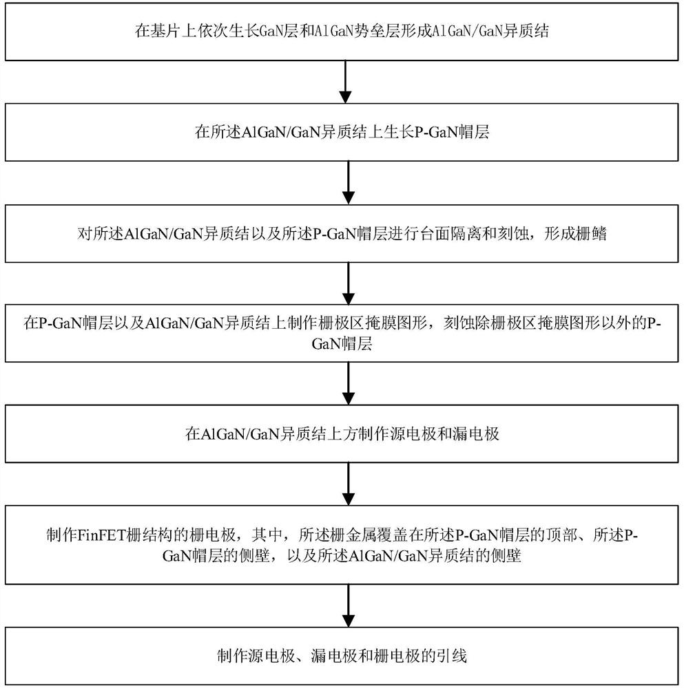
[0054] See figure 1 , figure 1 A schematic diagram of a method for manufacturing a FinFET enhanced device with a P-GaN cap layer provided by an embodiment of the present invention, including the following steps:

[0055] S1. Grow a GaN layer and an AlGaN barrier layer sequentially on the substrate to form an AlGaN / GaN heterojunction, where the substrate can be a sapphire substrate or a SiC substrate, and grow a GaN layer with a thickness of 1-2 μm on the selected substrate , and then grow an AlGaN barrier layer with a thickness of 10-20nm on the GaN layer, wherein the composition content of Al in the AlGaN barrier layer is 20%-30%; two-dimensional electrons are formed at the contact position between the GaN layer and the AlGaN barrier layer gas to obtain AlGaN / GaN heterojunction.

[0056] S2. Grow a P-GaN cap layer on the AlGaN / GaN heterojunction, grow a Mg-doped GaN cap layer with a thickness of 40-60 nm on the AlGaN barrier layer, and then heat the Mg-doped GaN cap layer an...

Embodiment 2

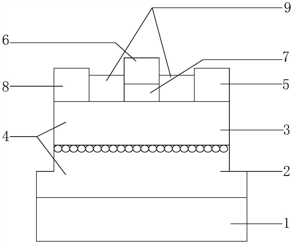
[0063] See figure 2 , figure 2 A schematic structural diagram of a FinFET enhancement device with a P-GaN cap layer provided by an embodiment of the present invention. Including: substrate 1, AlGaN / GaN heterojunction 4, SiN passivation layer 9, P-GaN cap layer 7, source electrode 8, drain electrode 5 and gate electrode 6;

[0064] The source electrode 8, the gate electrode 6, the drain electrode 5 and two pairs of SiN passivation layers 9 are located above the AlGaN / GaN heterojunction 4, wherein the first SiN passivation layer is located on the gate electrode 6 Between the source electrode 8, the second SiN passivation layer is located between the gate electrode 6 and the drain electrode 5, and the drain electrode 5 and the source electrode 8 are located at the AlGaN / GaN heterojunction 4 both sides;

[0065] The P-GaN cap layer 7 is located between the gate electrode 6 and the AlGaN barrier layer 3 , and the P-GaN cap layer 7 can effectively reduce the barrier height on o...

Embodiment 3

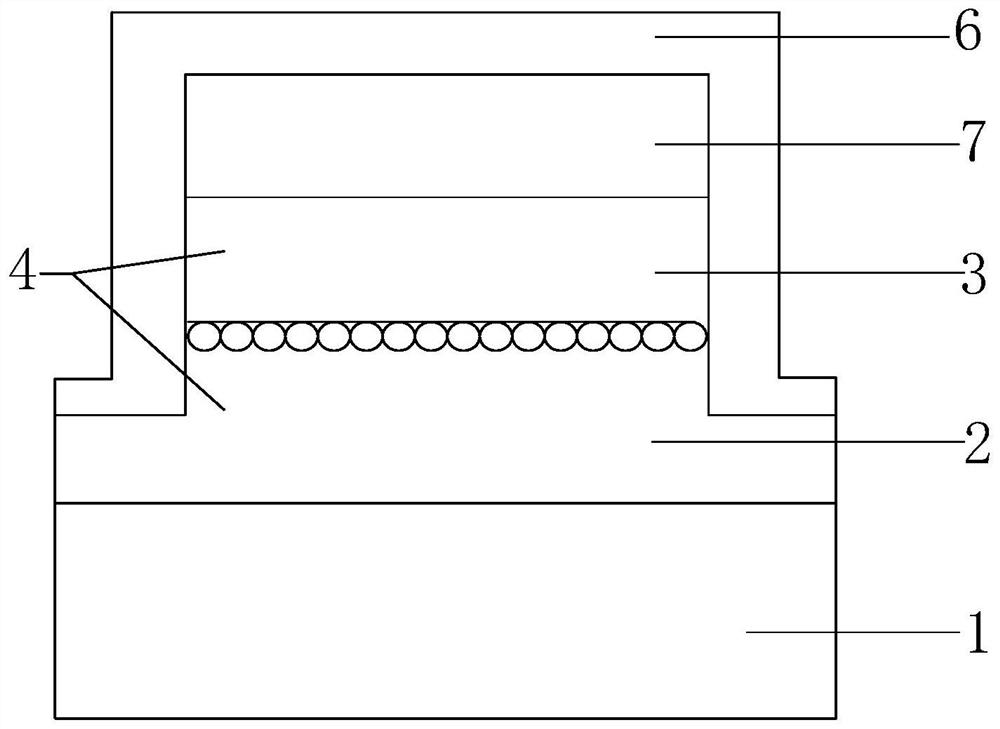
[0068] See Figure 4 , Figure 4 It is a schematic flow chart of the manufacturing process of a FinFET enhanced device with a P-GaN cap layer provided by an embodiment of the present invention. In this embodiment, on the basis of the above-mentioned embodiments, a detailed description will be focused on the manufacturing process of the device. Specifically, a FinFET enhancement device with a gate fin width of 30 nm and a P-GaN cap layer is manufactured.

[0069] Step 1. Using the MOCVD process to epitaxially grow the heterojunction:

[0070] 1.1. In this embodiment, SiC is selected as the substrate 1, and the GaN layer 2 with a thickness of 1 μm is grown on the SiC substrate substrate;

[0071] 1.2. Growing the AlGaN barrier layer 3 with a thickness of 10 nm on the GaN layer 2, wherein the Al composition is 25%, and forming two layers at the contact position between the GaN layer 2 and the AlGaN barrier layer 3 Dimensional electron gas to obtain the AlGaN / GaN heterojunctio...


PUM

PropertyMeasurementUnit
thicknessaaaaaaaaaa
thicknessaaaaaaaaaa
thicknessaaaaaaaaaa

Abstract

The invention relates to a FinFET enhanced device of a P-GaN cap layer and a manufacturing method. The manufacturing method comprises the steps of enabling a GaN layer and an AlGaN barrier layer sequentially to grow on a substrate to form an AlGaN / GaN heterojunction; enabling a P-GaN cap layer to grow on the heterojunction; performing mesa isolation and etching on the heterojunction to form a gatefin; forming a gate region mask pattern on the surfaces of the P-GaN cap layer and the heterojunction, and etching the P-GaN cap layer except the gate region mask pattern; manufacturing a source electrode and a drain electrode on two sides of the heterojunction; depositing gate metal in the region of the P-GaN cap layer to form a FinFET gate structure gate electrode, the gate metal covering the top and the sidewall of the P-GaN cap layer and covering the sidewall of the heterojunction; manufacturing an electrode lead. According to the device and the manufacturing method, a P-GaN cap layer structure is adopted, and a three-dimensional grid-controlled FinFET structure is combined, so that the transconductance and grid-control capabilities of the device are enhanced, and the threshold voltage and stability of the device are improved.

Description

technical field [0001] The invention belongs to the technical field of microelectronics, and in particular relates to a P-GaN cap layer FinFET enhanced device and a manufacturing method. Background technique [0002] In recent years, the third bandgap semiconductor represented by SiC and GaN has the characteristics of large bandgap, high breakdown electric field, high thermal conductivity, high saturated electron velocity and high concentration of two-dimensional electron gas at the heterojunction interface. It has received widespread attention. [0003] AlGaN / GaN heterojunction high electron mobility transistor HEMT has shown great advantages in high temperature devices and high power microwave devices. In recent years, due to the driving of high-voltage switches and high-speed circuits, GaN enhancement-mode devices have become another research hotspot. After the growth of the AlGaN / GaN heterojunction is completed, there is a large amount of two-dimensional electron gas 2...

Claims


Application Information

Patent Timeline
Patent Type & Authority Patents(China)
IPC IPC(8): H01L21/335H01L29/778H01L29/423H01L29/207
CPCH01L29/207H01L29/42356H01L29/66462H01L29/7786
Inventor 王冲黄泽阳何云龙郑雪峰马晓华郝跃
Owner XIDIAN UNIV
Why Eureka
Try Eureka