P-GaN/AlGaN/GaN enhanced device based on fin-shaped gate structure and manufacturing method thereof

A gate structure and enhanced technology, which is applied in the field of p-GaN/AlGaN/GaN enhanced devices and their fabrication, can solve the problems of not meeting the application requirements of GaN-based electronic devices, poor device reliability and stability, and small forward threshold voltage issues such as good process repeatability and temperature stability, enhanced gate control capability, and high threshold voltage

Inactive Publication Date: 2020-04-17
XIDIAN UNIV
View PDF6 Cites 4 Cited by
  • Summary
  • Abstract
  • Description
  • Claims
  • Application Information

AI Technical Summary

Problems solved by technology

However, the disadvantage of this method is that the gate leakage current is large, the forward threshold voltage is small, etc., and the reliability and stability of the devices manufactured by this method are poor, which cannot meet the application requirements of GaN-based electronic devices in the field of high-voltage switches.

Method used


Image

  • P-GaN/AlGaN/GaN enhanced device based on fin-shaped gate structure and manufacturing method thereof
  • P-GaN/AlGaN/GaN enhanced device based on fin-shaped gate structure and manufacturing method thereof
  • P-GaN/AlGaN/GaN enhanced device based on fin-shaped gate structure and manufacturing method thereof

Examples


Embodiment 1

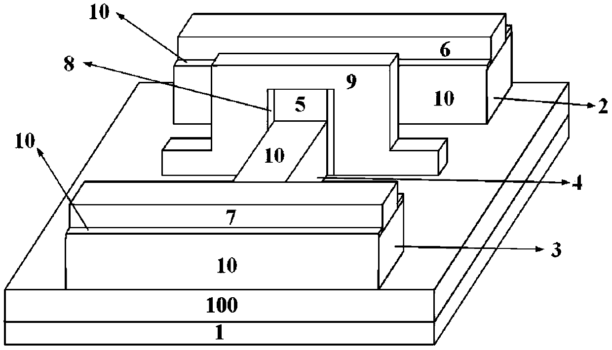
[0056] refer to figure 1 , figure 1 A schematic diagram of a p-GaN / AlGaN / GaN enhancement device based on a fin-shaped gate structure provided by an embodiment of the present invention.

[0057] An embodiment of the present invention provides a p-GaN / AlGaN / GaN enhanced device based on a fin-shaped gate structure, including:

[0058] substrate layer 1;

[0059] The source part 2 is located on one side of the upper layer of the substrate layer 1;

[0060] The drain part 3 is located on the other side of the upper layer of the substrate layer 1 and is opposite to the source part 2;

[0061] a Fin structure 4 located on the upper layer of the substrate layer 1 and located between the source part 2 and the drain part 3;

[0062] A cap layer 5, located on the upper layer in the middle of the Fin structure 4;

[0063] The source electrode 6 is located on the upper layer of the source part 2;

[0064] The drain electrode 7 is located on the upper layer of the drain part 3;

[00...

Embodiment 2

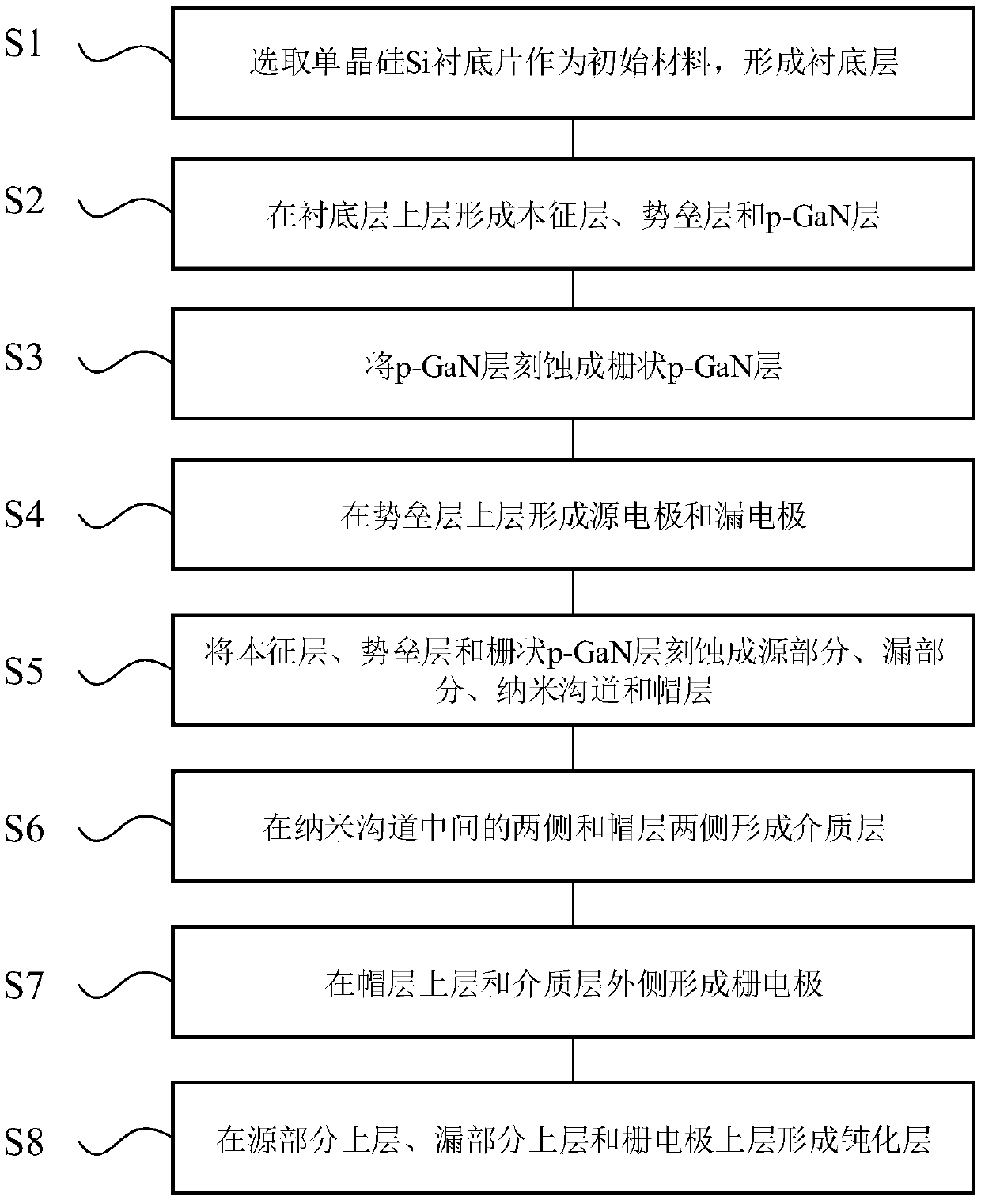
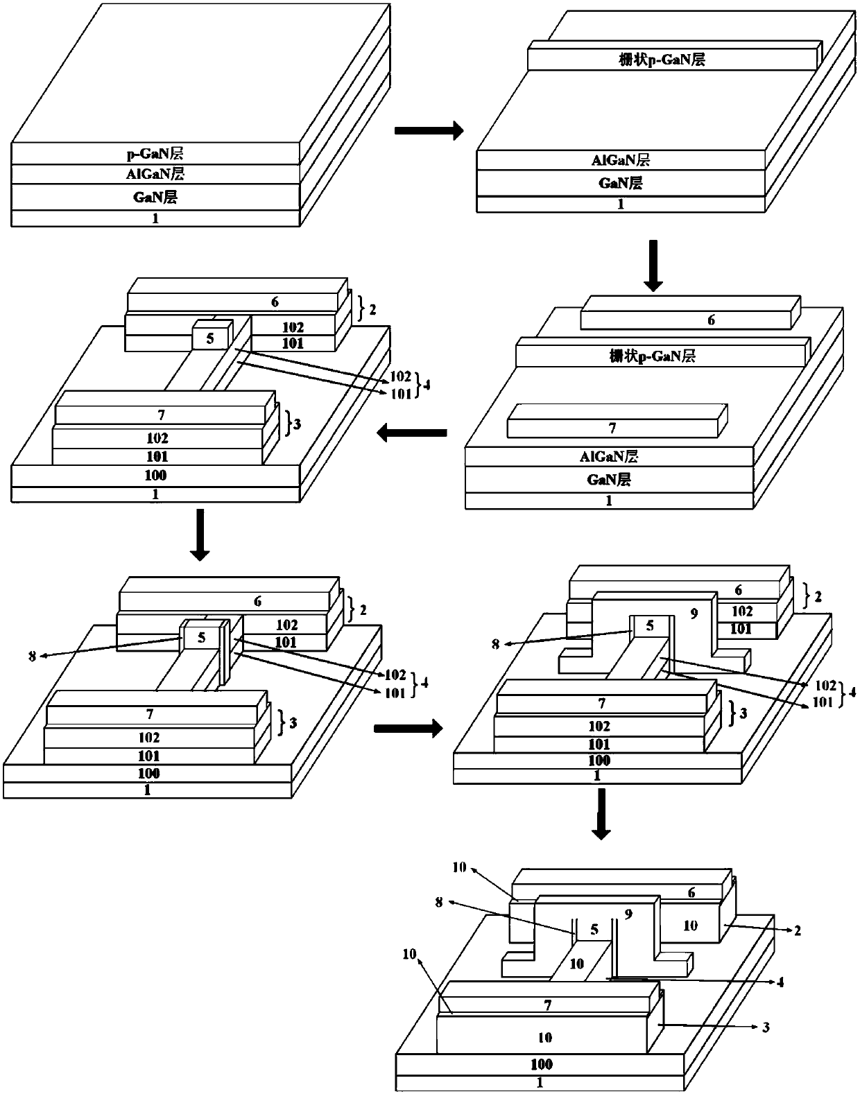
[0081] refer to figure 2 and image 3 , figure 2 A schematic flowchart of a manufacturing method of a p-GaN / AlGaN / GaN enhancement device based on a fin-shaped gate structure provided by an embodiment of the present invention; image 3 It is a schematic diagram of a manufacturing method of a p-GaN / AlGaN / GaN enhancement device based on a fin-shaped gate structure provided by an embodiment of the present invention.

[0082] Another embodiment of the present invention provides a method for manufacturing a p-GaN / AlGaN / GaN enhanced device based on a fin-shaped gate structure, including:

[0083] S1. Selecting a single crystal silicon Si substrate as an initial material to form a substrate layer 1;

[0084] S2, forming a GaN layer, an AlGaN layer and a p-GaN layer on the substrate layer 1;

[0085] S3. Etching the p-GaN layer into a gate-shaped p-GaN layer;

[0086] S4, forming a source electrode 6 and a drain electrode 7 on the upper layer of the AlGaN layer;

[0087] S5, et...


PUM

PropertyMeasurementUnit
Thicknessaaaaaaaaaa
Thicknessaaaaaaaaaa
Thicknessaaaaaaaaaa

Abstract

The invention relates to a p-GaN / AlGaN / GaN enhanced device based on a fin-shaped gate structure. The p-GaN / AlGaN / GaN enhanced device comprises a substrate layer, a source part which is positioned on one side of the upper layer of the substrate layer, a drain part which is positioned on the other side of the upper layer of the substrate layer and is opposite to the source part, a Fin structure which is located on the upper layer of the substrate layer and located between the source part and the drain part, a cap layer which is positioned on the upper layer in the middle of the Fin structure, asource electrode on the upper layer of the source part, a drain electrode positioned on the upper layer of the drain part, dielectric layers located on the two sides of the middle of the Fin structureand the two sides of the cap layer, a gate electrode positioned on the upper layer of the cap layer and outside the dielectric layer, and a passivation layer coating the source part, the drain part and the Fin structure. According to the device provided by the invention, the gate can control the channel from three directions, so that the gate leakage current is effectively reduced; in addition, the cap layer and the Fin structure side gate are used for exhausting the channel 2DEG, so that the forward threshold voltage is improved.

Description

technical field [0001] The invention belongs to the field of semiconductor technology and semiconductor manufacturing, and in particular relates to a p-GaN / AlGaN / GaN enhanced device based on a fin-shaped gate structure and a manufacturing method thereof. Background technique [0002] In recent years, the third-generation wide-bandgap semiconductors represented by SiC and GaN have the characteristics of large bandgap, high breakdown electric field, high thermal conductivity, high saturated electron velocity, and high two-dimensional electron gas concentration at the heterojunction interface. , has gradually become a research hotspot at home and abroad. HEMTs (High Electron Mobility Transistors) made of AlGaN / GaN heterojunctions have shown unique advantages in high-temperature devices and high-power microwave devices. [0003] Generally speaking, after the growth of the AlGaN / GaN heterojunction is completed, there will be a large amount of 2DEG (two-dimensional electron gas) ...

Claims


Application Information

Patent Timeline
IPC IPC(8): H01L29/778H01L29/423H01L21/335
CPCH01L29/42316H01L29/66462H01L29/778
Inventor 何云龙马晓华王冲郑雪峰郝跃
Owner XIDIAN UNIV
Why Eureka
Try Eureka