Photoconductive bolometer infrared detector

a bolometer and infrared detector technology, applied in the field of infrared light detectors, can solve the problems of thermal noise limitation of ideal bolometer performance, poor out-of-band responsivity, and conventional bolometer designed for maximum efficiency in the lwir normally has poor responsivity in the lwir, so as to enhance the operation of the enhanced mid-wave infrared (mwir) and the effect of thermal absorption of incident radiation

Active Publication Date: 2007-08-28
NORTHROP GRUMMAN SYST CORP
View PDF6 Cites 13 Cited by
  • Summary
  • Abstract
  • Description
  • Claims
  • Application Information

AI Technical Summary

Benefits of technology

[0010]A photoconductive bolometer infrared detector is provided. The photoconductive bolometer infrared detector uses a detector material that has a resistance changed due to photo-excitation and thermal-excitation from an incident radiation in the infrared range. The resistance changes caused by photo-excitation and the thermal excitation are additive for this detector material. The detector material is suspended over a substrate by a gap of one quarter wavelength of the incident radiation, such that the thermal absorption of the incident radiation can be enhanced. In one embodiment, the detector material includes lead selenide (PbSe) that has a thermal coefficient of resistance as high as 3.45%° C.−1, which is about 60% higher than that of vanadium oxide that has been widely used as the detector material in the conventional microbolometers. This detector structure allows dual band uncooled or moderately cooled operation. By using PbSe as the detector material, largely enhanced mid-wave infrared (MWIR) operation is enabled over a standard uncooled micro-bolometer tuned to the LWIR, and high temperature dual band MWIR and long-wave infrared (LWIR) operation is enabled as compared to quantum well or HgCdTe detectors that must be cooled to cryogenic temperatures.
[0012]In one embodiment, the PbSe detector layers are selectively sensitized, such that the medium-wavelength radiation can be detected by the sensitized detectors, while the long-wavelength radiation can be obtained by interpolation between outputs of the sensitized and unsensitized detector layers. Alternatively, high pass filters or medium-wavelength infrared absorbers may be applied to selective detector layers to achieve the same effect.

Problems solved by technology

Ideal bolometer performance is limited by thermal noise and has a responsivity proportional to the bias current and the TCR.
If the detector is designed for maximum efficiency in the LWIR, its out-of-band responsivity will be poor.
Therefore, the conventional photoconductive infrared detector, though having sufficient responsivity in the MWIR, often requires a cryogenic cooling system to prevent the optical signal from being buried by the thermally excited electrons or noise.
The conventional bolometer designed for maximum efficiency in the LWIR normally has poor responsivity in the LWIR.

Method used


Image

  • Photoconductive bolometer infrared detector
  • Photoconductive bolometer infrared detector
  • Photoconductive bolometer infrared detector

Examples


Embodiment Construction

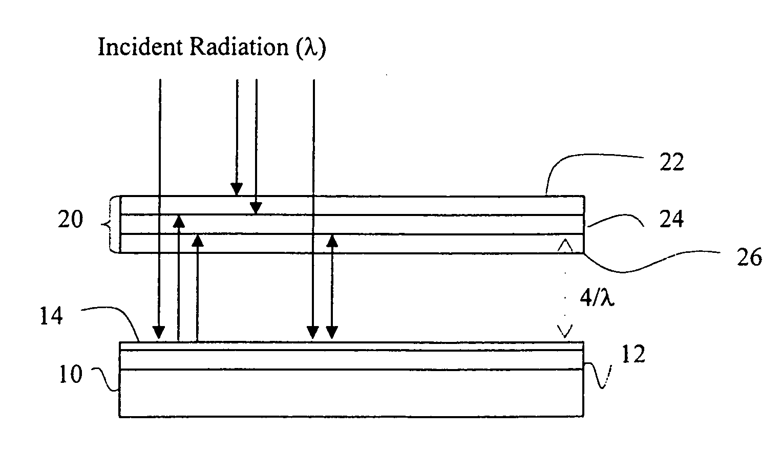
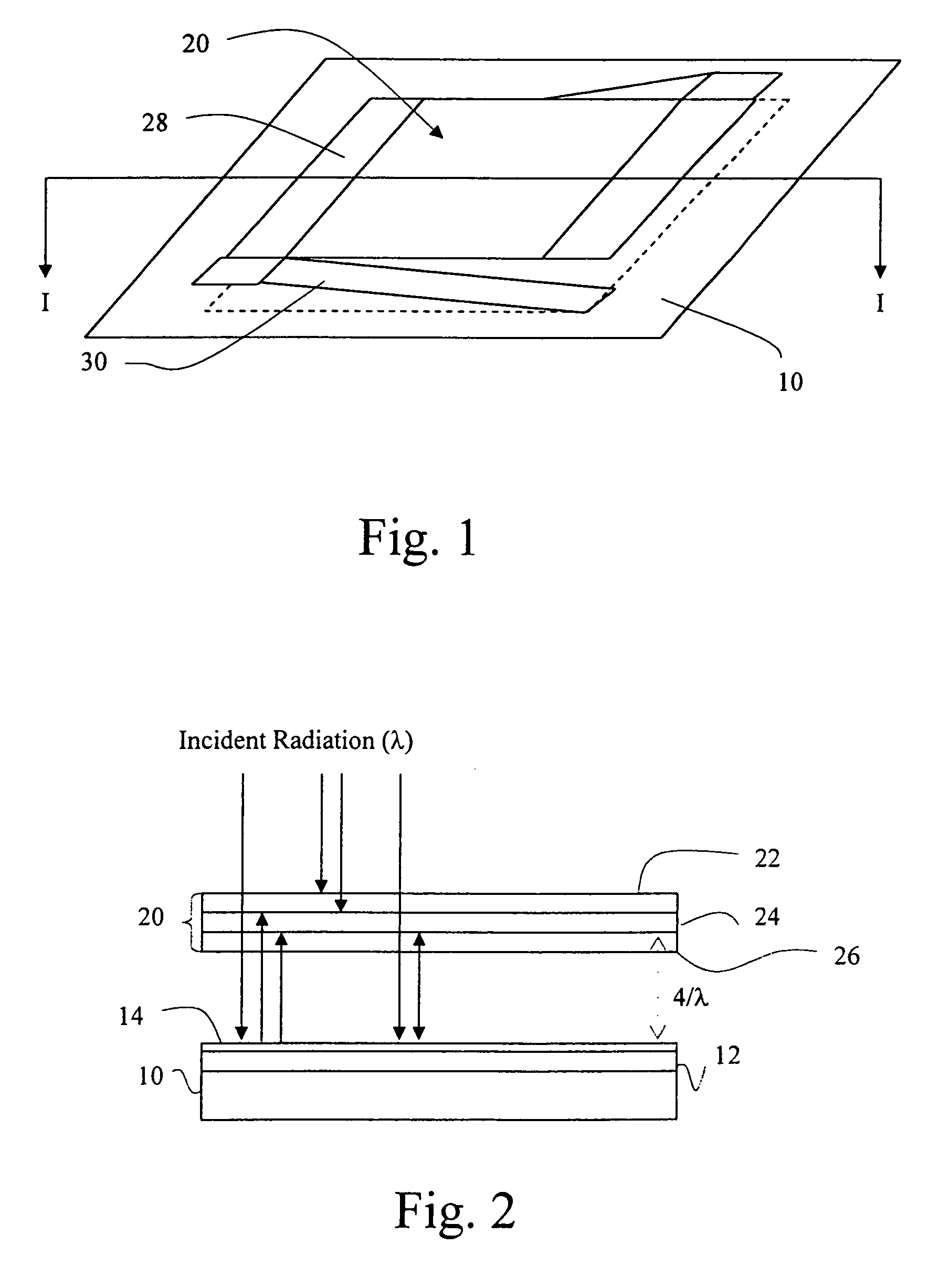
[0021]Referring now to the drawings wherein the showings are for the purpose of illustrating preferred embodiments of the present invention only, and not for the purposes of limiting the same, FIGS. 1 and 2 are the perspective and cross-sectional views, respectively, of an exemplary microbolometer infrared detector using lead selenide (PbSe) as the detector material. As shown, the microbolometer infrared detector 40 includes an active detector area 20 suspending over a substrate 10, a pair of conductive or metal contacts 28 at two opposing edges of the active detector area 20, and a pair of legs 30 extending from the substrate 10 to support the active detector area 20 over the substrate 10. The active detector area 20 includes a lead selenide layer 22 serving as a detector layer, a preferred but optional layer of absorber 24, and a protective layer 26. The protective layer 26 includes a silicon oxide layer, for example. The substrate 10 is preferably fabricated from materials such a...


PUM


Abstract

A photoconductive bolometer infrared detector using a detector material that has a resistance changed due to photo-excitation and thermal-excitation from an incident radiation in the infrared range. The resistance changes caused by photo-excitation and the thermal excitation are additive for this detector material. The detector material is suspended over a substrate by a gap of one quarter wavelength of the incident radiation, such that the thermal absorption of the incident radiation can be enhanced. Preferably, the detector material is lead selenide that has a thermal coefficient of resistance as high as 3.45%° C.−1, which is about 60% higher than that of vanadium oxide that has been widely used as the detector material in the conventional microbolometers. This detector structure allows dual band uncooled or moderately cooled operation. In the case of the use of PbSe as the detector material, largely enhanced MWIR operation is enabled over a standard uncooled micro-bolometer tuned to the LWIR, and high temperature dual band MWIR and LWIR operation is enabled as compared to quantum well or HgCdTe detectors that must be cooled to cryogenic temperatures.

Description

CROSS-REFERENCE TO RELATED APPLICATIONS[0001]Not ApplicableSTATEMENT RE: FEDERALLY SPONSORED RESEARCH / DEVELOPMENT[0002]Not ApplicableBACKGROUND OF THE INVENTION[0003]The present invention relates in general to an infrared light detector, and more particularly, to an infrared detector that is a photoconductive bolometer having good responsivity in the short or mid-wave infrared and also in the long-wave infrared.[0004]When light strikes special types of materials, a voltage may be generated, a change in electrical resistance may occur, or electrons may be ejected from the material surface. As long as the light is present, the condition continues. These special types of materials are often used as optical detectors to detect the characteristics of an optical signal. Two broad classes of infrared optical detectors include photon detectors and thermal detectors. A photon detector generates free electrons when the incident radiation excites electrons from the valence band to the conducti...

Claims


Application Information

Patent Timeline
Patent Type & Authority Patents(United States)
IPC IPC(8): G01J5/00
CPCG01J5/20
Inventor KAUFFMAN, CHRISTOPHER L.YOO, SUNG-SHIKBEYSTRUM, TIMOTHY R.
Owner NORTHROP GRUMMAN SYST CORP
Why Eureka
Try Eureka