Integrated optical isolator array

a technology of optical isolators and arrays, applied in the field of non-reciprocal optical devices, can solve the problems of high cost and production volume limitations, difficulty in automating the placement and alignment of optical fibers and any separate collimating elements, and increase manufacturing costs, so as to improve the quality of optical fibers and reduce noise , the effect of reducing the cost of manufactur

Inactive Publication Date: 2007-08-28
BROADEX TECH UK LTD
View PDF17 Cites 32 Cited by
  • Summary
  • Abstract
  • Description
  • Claims
  • Application Information

AI Technical Summary

Benefits of technology

[0011]The invention further encompasses a doped fiber amplifier array architecture employing an integrated circulator array of the foregoing description. The architecture includes an array of input fibers each carrying an input signal to be amplified, and an array of output fibers each carrying an amplified output signal. Each input fiber is coupled to a corresponding circulator structure via a first port thereof, and each output fiber is coupled to a corresponding circulator structure via a third port thereof. An array of doped fibers are optically coupled at their first ends to corresponding second ports of the circulator structures and receive pump light through their second ends. An input light signal entering a circulator structure is routed to the second port, where it is then coupled into the first end of the corresponding doped fiber. The light signal is amplified as it travels along the length of the doped fiber. A wavelength selective reflector located at the second end of the doped fi

Problems solved by technology

Manufacturing of such isolators involve numerous assembly and manufacturing steps (most of which must be performed manually), resulting in high costs and limitations in production volume.
The approach described in the aforementioned Pan patent does offer certain advantages over existing single-channel designs, but has several problems associated with its implementation.
These problems include a need to utilize non-standard fibers having thick (>200 μm) claddings to prevent exc

Method used


Image

  • Integrated optical isolator array
  • Integrated optical isolator array
  • Integrated optical isolator array

Examples


Embodiment Construction

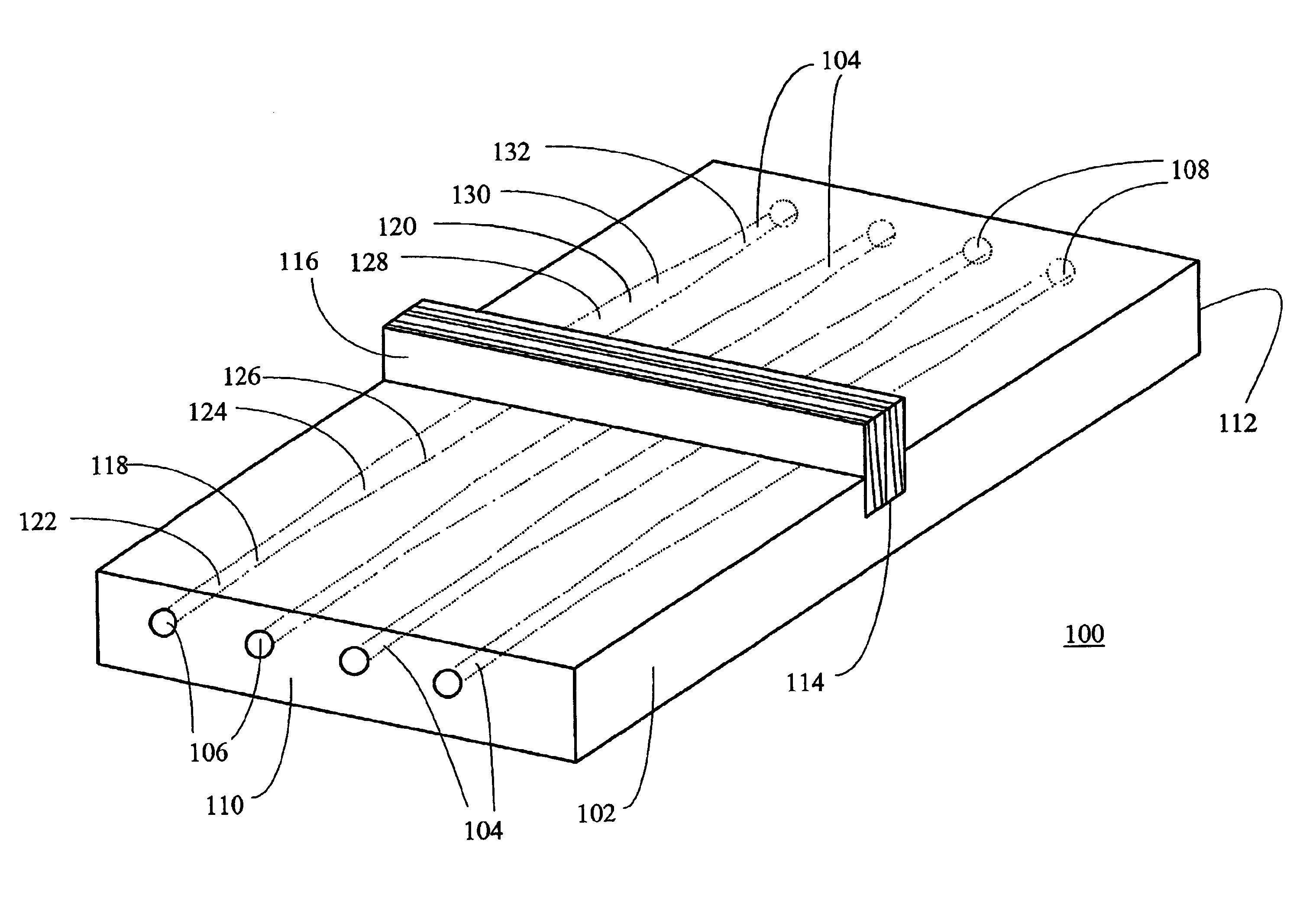
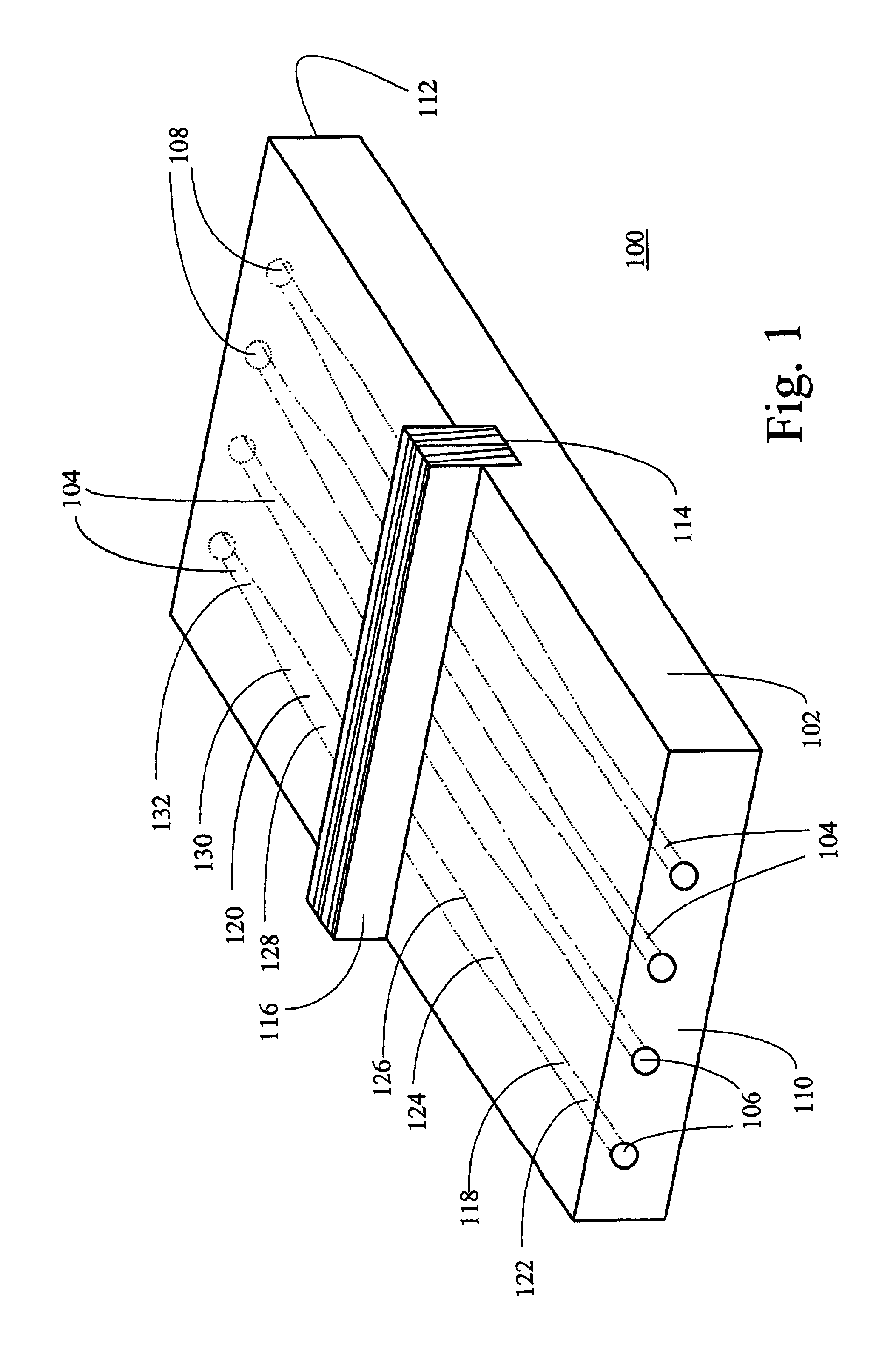
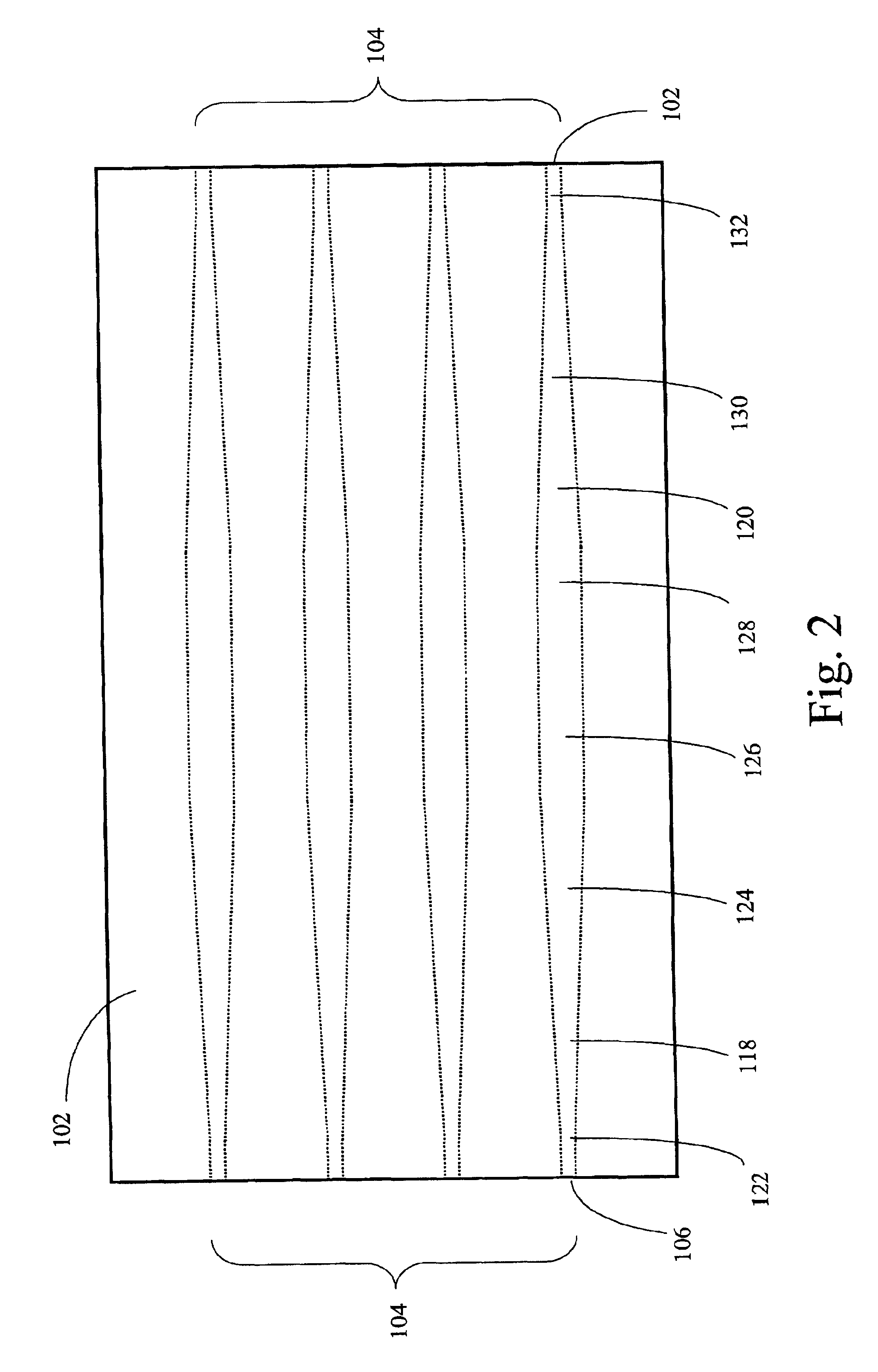
[0021]FIG. 1 illustrates the general structure of an integrated isolator array 100 in accordance with a first embodiment of the invention. Isolator array 100 includes an optical substrate 102 having a plurality of laterally spaced apart waveguides (individually and collectively denoted as 104) formed therein. The waveguides terminate at input and output ports 106 and 108 located at the opposite end faces 110 and 112 of substrate 102. The waveguides may be optically coupled via the input and output ports to corresponding arrays of input and output optical fibers (not shown), which carry input and output light signals. Precise positioning and alignment of the optical fiber arrays relative to the input and output ports may be accomplished by use of v-grooved or similar structures, which are known in the art and will not be discussed herein.

[0022]Optical substrate 102 may be fabricated from lithium niobate, a glass, or other material (or combination of materials) which is optically tran...


PUM


Abstract

An integrated isolator array is provided having a plurality of waveguides fabricated in a planar optical substrate, each waveguide having input and output sections. An isolator subassembly is received within a transverse trench formed in the substrate between the input and output sections such that it intersects the optical paths of the waveguides. The isolator subassembly, which may consist of layers of Faraday rotator material sandwiched between layers of birefringent crystal material, permits the forward passage of light from the input sections to the output sections of the waveguides while preventing the backward passage of light from the output to the input sections. Each waveguide input section is preferably adapted with a mode-expanding input taper to collimate light propagating through the waveguide. Similarly, each output section is preferably adapted with a mode-reducing output taper to reduce the mode size of forward-traveling light to match that of an output fiber, as well as to collimate light traveling backward within the output section.

Description

CROSS-REFERENCE TO RELATED APPLICATIONS[0001]This application is related to the following commonly assigned applications filed on even date herewith: U.S. application Ser. No. 10 / 073,814 entitled “Integrated Optical Circulator Array” by inventors Hehlen et al., and U.S. application Ser. No. 10 / 073,754 now U.S. Pat. No. 6,560,387 entitled “Doped Fiber Amplifier Utilizing Integrated Circulator Array” by inventors Hehlen et al.BACKGROUND[0002]1. Field of the Invention[0003]The present invention relates generally to nonreciprocal optical devices, and more particularly to arrays of nonreciprocal devices, such as isolators and circulators, integrated on a common planar optical substrate.[0004]2. Description of the Prior Art[0005]Nonreciprocal optical devices, such as optical isolators and optical circulators, are essential components of optical communication systems. Optical isolators pass light propagating in a forward direction while inhibiting the propagation of light in a backward dir...

Claims


Application Information

Patent Timeline
IPC IPC(8): G02B6/12G02B6/28
CPCG02B6/126G02B6/4208G02F1/0955G02B6/4249
Inventor HEHLEN, MARKUS P.BISCHEL, WILLIAM K.
Owner BROADEX TECH UK LTD
Why Eureka
Try Eureka