Semiconductor integrated circuit device with boundary scan test and design automation apparatus, boundary scan test method and program

a technology of integrated circuits and test methods, applied in the direction of error detection/correction, cad circuit design, instruments, etc., can solve the problems of reducing the accuracy and reliability of tests, increasing the degree of waveform depression at the far end, and increasing the delay of test signals, so as to improve the reliability and precision of tests, reduce design and development costs, and facilitate small production.

Inactive Publication Date: 2007-08-28
RENESAS ELECTRONICS CORP
View PDF15 Cites 19 Cited by
  • Summary
  • Abstract
  • Description
  • Claims
  • Application Information

AI Technical Summary

Benefits of technology

[0022]The present invention has an advantage such that a semiconductor integrated circuit, such as ASIC, which is constructed by using the test facilitating design scheme can suppress a delay of a test signal and waveform depression caused by an empty cell and can ensure delay adjustment, thereby improving the reliability and precision of a test.
[0023]Further, as the present invention can permit c...

Problems solved by technology

As the chip size increases, therefore, the wiring length becomes longer and the delay of the test signals increases because of factors, such as the wiring resistance and floating capacitance, thereby increasing the degree of wavefo...

Method used


Image

  • Semiconductor integrated circuit device with boundary scan test and design automation apparatus, boundary scan test method and program
  • Semiconductor integrated circuit device with boundary scan test and design automation apparatus, boundary scan test method and program
  • Semiconductor integrated circuit device with boundary scan test and design automation apparatus, boundary scan test method and program

Examples


Embodiment Construction

[0034]A preferred embodiment of the present invention is described below with reference to the accompanying drawings.

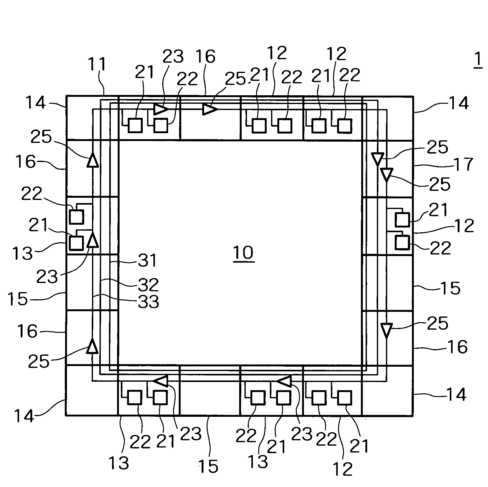
[0035]FIG. 3 is a diagram illustrating the schematic structure of a semiconductor integrated circuit according to one embodiment of the present invention. Referring to FIG. 3, empty cells each having a repeater circuit are adequately laid out in an empty cell area where no I / O cells are laid out in an I / O area in the peripheral portion of a chip where I / O cells are laid out in this embodiment. Specifically, wirings 31, 32 and 33 for transferring a test signal to a plurality of I / O cells in the I / O area are provided in the I / O area over a plurality of I / O cells in the layout direction of the I / O cells to form global wirings. Of those empty cells over which the wirings 31, 32 and 33 path, an empty cell A 16 and an empty cell B 17 each having a repeater circuit 25 that constitute a transfer path for a test signal, receives the test signal and outputs the test signal are ...


PUM


Abstract

An area for layout of a plurality of I/O cells (called an “I/O area”) is provided in the peripheral portion of a chip and signal wirings for transferring test signals to the I/O cells are provided in the layout direction of the I/O cells. At least one empty cell provided in the I/O area at a position where I/O cells are not provided has a repeater circuit which constitutes a transfer path for the test signal. The repeater circuit receives the test signal and outputs the test signal. This structure provides a suitable semiconductor integrated circuit device adaptable for an ASIC or the like, which can adjust the delay of a test signal to be transferred along the chip's peripheral portion by suppressing an increase in the delay and degradation in waveform depression.

Description

BACKGROUND OF THE INVENTION[0001]1. Field of the Invention[0002]The present invention relates to a semiconductor integrated circuit device, and, more particularly, to a semiconductor integrated circuit device, and a design automation method, apparatus and program which employ a test facilitating design technology.[0003]2. Description of the Related Art[0004]Boundary scan (JTAG) which is one scheme for test facilitating design is standardized in 1990 as described in IEEE std 1149.1-1990 Standard Test Access Port and Boundary-Scan Architecture and is a test method mainly aiming at checking wiring connection between LSIs.[0005]FIG. 1 is a diagram illustrating the schematic structure of a typical boundary-scan circuit (see, for example, “Fundamentals and Application of JTAG Test” by Kazumi Sakamaki, p 24, FIG. 2-2, CQ Publication Co., Ltd., Dec. 1, 1998). A boundary-scan register has a multiplexer M1, a flip-flop F1, a flip-flop F2, and a multiplexer M2. The multiplexer M1 receives a se...

Claims


Application Information

Patent Timeline
IPC IPC(8): G06F17/50G01R31/28G01R31/3185H01L21/82H01L21/822H01L27/04
CPCG01R31/318538G06F17/5068G06F30/39
Inventor KUGE, HIROYOSHIOHARA, YOSHIHIRO
Owner RENESAS ELECTRONICS CORP
Why Eureka
Try Eureka