Non-volatile semiconductor memory

a semiconductor memory and non-volatile technology, applied in semiconductor devices, digital storage, instruments, etc., can solve the problems of increasing the number of masks, lowering the operating voltage, and increasing the production steps, so as to reduce the voltage, the voltage margin at the time of the read operation is enlarged, and the electrical reliability such as the charge holding characteristic and data rewriting characteristic is improved

Inactive Publication Date: 2007-09-04
SONY CORP
View PDF12 Cites 2 Cited by
  • Summary
  • Abstract
  • Description
  • Claims
  • Application Information

AI Technical Summary

Benefits of technology

[0022]Summarizing the effects of the invention, according to the non-volatile semiconductor memory of the present invention, operation where a short channel effect occurs at the time of a write operation, but does not occur at the time of a read operation becomes possible. For this reason, compared with a case where a short channel effect does not occur, the injection of a charge at the time of a write operation starts from a threshold (torelance) voltage on the non-write side, so injection of a larger amount of charge is possible under the same voltage conditions. As a result, the difference between the threshold voltage in the written state and the threshold voltage in the non-written state is enlarged, the voltage margin at the time of the read operation is enlarged by that amount, and the electrical reliability such as the charge holding characteristic and data rewrite characteristic is improved. On the other hand, the voltage necessary for injecting the same amount of charge is lowered, so a reduction of the voltage is possible.
[0023]Further, according to the non-volatile semiconductor memory of the present invention, a write operation is possible from the state where the threshold voltage level at the time of commencement of the injection of the charge at the time of a write operation (first level) is at the non-write side from the threshold voltage level of the memory transistor in the non-written state at the time of a read operation (second level). For this reason, it is possible to make the amount of injected charge larger with the same application voltage in comparison with an ordinary case where the charge is injected from the second level. As a result, the difference between the threshold voltage in the written state and the threshold voltage in the non-written state is enlarged, the voltage margin at the time of the read operation is enlarged by that amount, and the electrical reliability such as the charge holding characteristic and the data rewrite characteristic is improved. On the other hand, the voltage necessary for injecting the same amount of charge is lowered, so a reduction of the voltage is possible.

Problems solved by technology

This leads to an increase of the production steps and an increase of the number of masks.
In this way, lowering the operating voltage is an important issue in combination non-volatile memories.
The fact that the window immediately after the write operation becomes smaller together with the operating voltage is becoming an obstacle (hurdle) to lowering the voltage.

Method used


Image

  • Non-volatile semiconductor memory
  • Non-volatile semiconductor memory
  • Non-volatile semiconductor memory

Examples


first embodiment

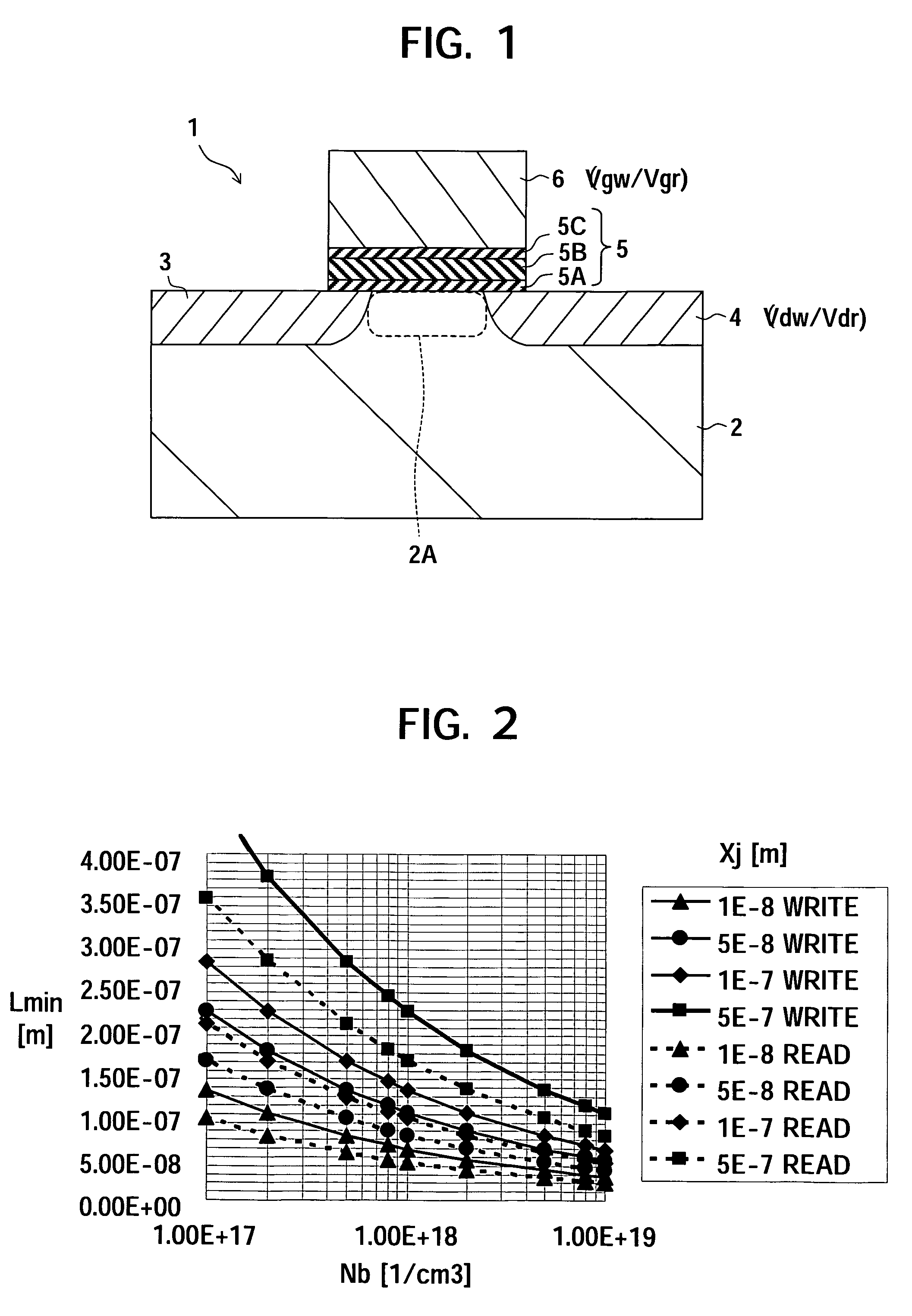
[0056]FIG. 1 shows the structure of a memory device on which a first embodiment of the present invention is predicated. The device structure is basically the same as an ordinary MONOS type memory transistor in the point of the source side and the drain side being symmetric, so a detailed explanation will be omitted here. Further, also the method of production is substantially identical to that of an ordinary MONOS type memory transistor, so the explanation here will be omitted as well. However, it is sometimes desirable to optimize the structural parameters (for example, the channel length). This point will be explained later.

[0057]In FIG. 1, notation (reference) 1 shows a memory transistor. In the same way, notation 2 shows a semiconductor substrate, notation 2A shows a P-type semiconductor region in which a channel is formed (hereinafter referred to as a “channel formation region”), notation 3 shows an N-type source region, notation 4 shows an N-type drain region, notation 5 shows...

second embodiment

[0106]The second embodiment relates to the design of the structure of a memory transistor able to enlarge the settable range of the channel length and able to make the short channel effect at the time of a write operation further larger by that. Specifically, in the present embodiment, an asymmetric structure is given to the source side and the drain side of the memory transistor and the direction of the drain voltage is reversed at the time of a write operation and the time of a read operation so as to make the memory transistor operate reversing the asymmetry.

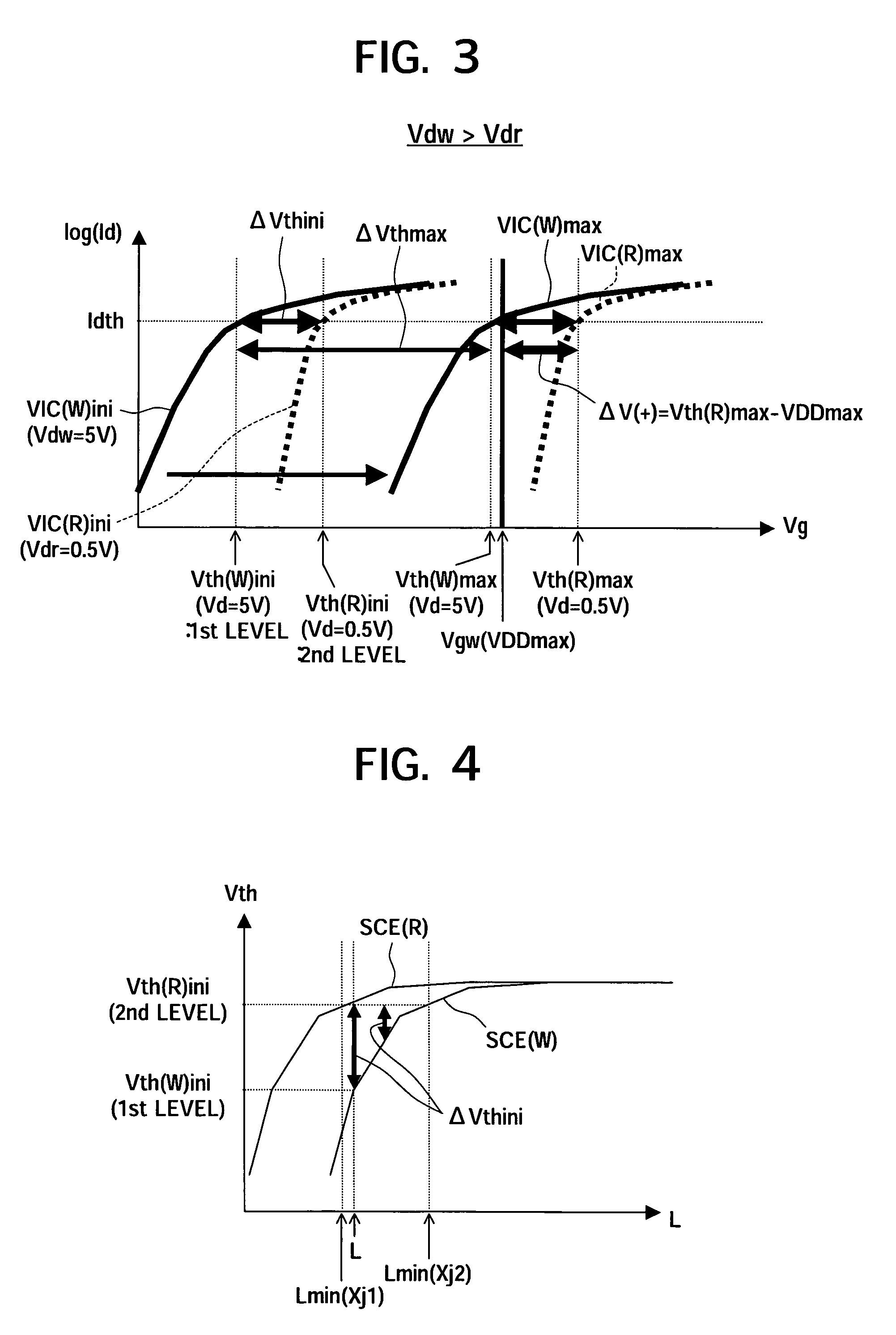
[0107]Note that, in the present embodiment, only the structure of the memory transistor and the direction of the drain voltage are different. The description concerning the basic operation described in the first embodiment and further the threshold voltage change and the gate length setting using equation (1) to inequality (10-1) and inequality (10-2) can be applied as is in the present embodiment.

[0108]The above equation (7)...

example 1

STRUCTURAL EXAMPLE 1

[0121]Structural Example 1 relates to a device structure forming two second conductivity type regions (S / D impurity regions) having different depths by impurity diffusion layers.

[0122]FIG. 6 is a sectional view of a memory transistor of Structural Example 1. In the first embodiment, the source region 3 and the drain region 4 are simultaneously formed, therefore they have substantially equal thicknesses (depths of the bottom junction from the surface of the channel formation region 2A) (refer to FIG. 1). Here, one of the two S / D impurity regions 7 and 8 corresponding to the source region 3 and the drain region 4, i.e., here, the S / D impurity region 8, is made thicker. The thick S / D impurity region 8 functions as the drain at the time of a write operation, and the thin S / D impurity region 7 functions as the drain at the time of a read operation.

[0123]FIGS. 7A to 7C to FIGS. 11A to 11C are sectional views of states in the formation of Structural Example 1. First, in...


PUM


Abstract

A non-volatile semiconductor memory having a memory transistor including a stacked-layer film formed between a semiconductor substrate and a gate electrode and having a charge storage ability, a first conductivity type region of the semiconductor substrate in which a channel is formed under the control of the gate electrode via the stacked-layer film, and two second conductivity type regions formed at the semiconductor substrate sandwiching the first conductivity type region therebetween, the memory transistor having a channel length L which is between channel lengths L1 and L2. with the channel length L1 being estimated as the boundary of occurrence of a short channel effect at the time of a write operation and the channel length L2 the time of a read operation, with the channel length L1 being different from the channel length L2.

Description

CROSS REFERENCES TO RELATED APPLICATIONS[0001]This application claims the benefit of Japan Patent Application No. P2004-178364, filed Jun. 16, 2004, the contents of which are hereby incorporated herein by reference in their entirety.BACKGROUND OF THE INVENTION[0002]1. Field of the Invention[0003]The present invention relates to a non-volatile semiconductor memory for storing data by injecting a charge into a stacked-layer film having a charge storage ability.[0004]2. Description of the Related Art[0005]In the past, a non-volatile memory injecting a charge into a stacked-layer film having a charge storage ability under predetermined voltage conditions desirably has used a high voltage for write and erase operations. Further, such a non-volatile memory has sometimes been combined with a logic circuit on the same IC. Below, such an IC is referred to as a “combination non-volatile memory”. In a combination non-volatile memory, a voltage higher than the voltage for driving the logic circ...

Claims


Application Information

Patent Timeline
Patent Type & Authority Patents(United States)
IPC IPC(8): H01L29/76G11C11/34H01L21/28H01L29/10H01L29/792
CPCH01L21/28282H01L29/1033H01L29/792H01L29/40117
Inventor KOBAYASHI, TOSHIOTOMIIE, HIDETO
Owner SONY CORP
Why Eureka
Try Eureka