Method of fabricating semiconductor device having multilayer wiring structure

a semiconductor device and wiring structure technology, applied in semiconductor devices, semiconductor/solid-state device details, electrical devices, etc., can solve the problems of difficult processing techniques, difficult to obtain desired insulating properties, and position margins, and achieve the effect of stable electric characteristics

Inactive Publication Date: 2007-09-11
KK TOSHIBA
View PDF11 Cites 2 Cited by
  • Summary
  • Abstract
  • Description
  • Claims
  • Application Information

AI Technical Summary

Benefits of technology

[0018]Therefore, an object of the present invention is to provide a semiconductor device in which a sufficient insulation distance can be ensured between the upper wiring layer and the adjacent contact plug in consideration of occurrence of misalignment in the lithography process, and a stable electric characteristic can be achieved and yet, a stable process can be provided so that embeddability the burying performance of the interlayer insulating film stacked on the upper layer can be prevented from being reduced, and a method of fabricating the semiconductor device.

Problems solved by technology

Such a reduction in the distance between each via hole and the metal wiring further reduces a positioning margin in a lithography process, which renders the processing technique difficult.
In addition, since a distance between adjacent wiring patterns is reduced, it becomes difficult to obtain a desired insulating property.
When a sufficient distance of insulation is not obtained, there arises a problem of failure due to short circuit such as dielectric breakdown or direct short circuit or a problem of parasitic capacitance, resulting in a difficulty in achieving a stable device operation.
Consequently, there is a possibility of occurrence of a short circuit or an increase in the parasitic capacitance.
However, the reduction in the circuit design rules makes it difficult to obtain an insulation distance and at the same time, it is quite difficult to carry out further reconsideration of the positioning specification in view of the device performance.
Further, variations in the diameter of the via hole also make it difficult to obtain a stable distance between insulators.
As a result, a desired operation of the device cannot be achieved.

Method used


Image

  • Method of fabricating semiconductor device having multilayer wiring structure
  • Method of fabricating semiconductor device having multilayer wiring structure
  • Method of fabricating semiconductor device having multilayer wiring structure

Examples


first embodiment

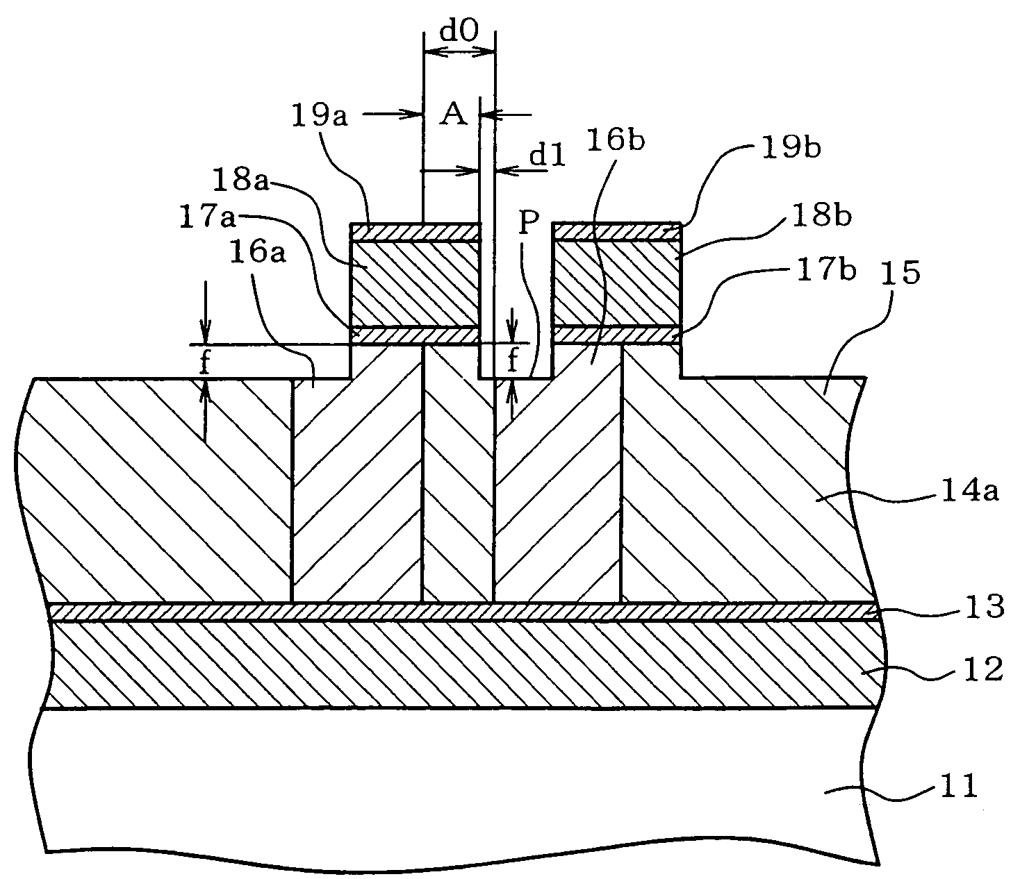
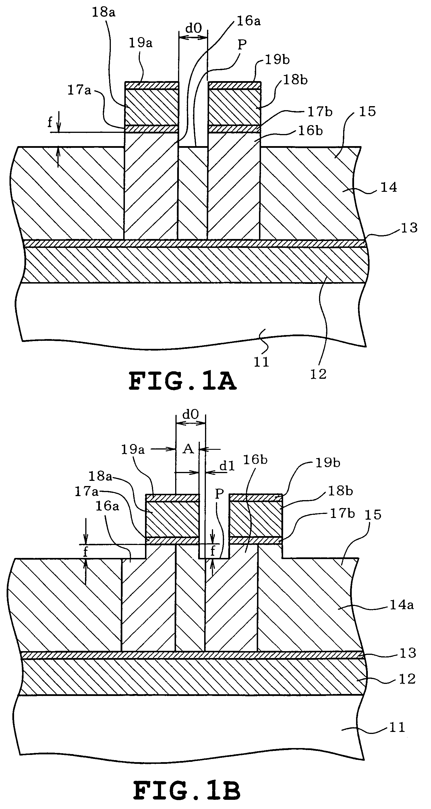
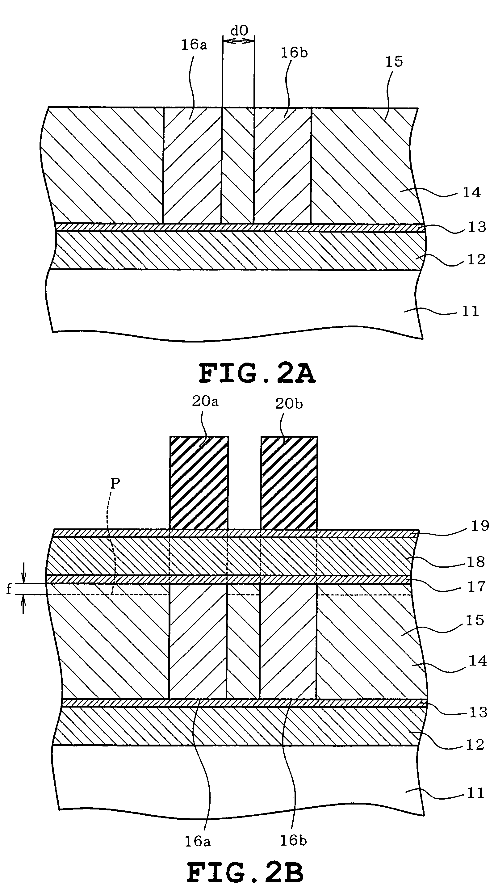
[0032]Several embodiments of the present invention will be described with reference to the accompanying drawings. FIGS. 1A to 3 illustrate the invention. Each figure shows a typical section of a part of the multilayer wiring structure. Dimensions do not sometimes agree to the actual dimensions for the sake of easiness in explanation.

[0033]FIGS. 1A and 1B show one layer of the multilayer wiring structure in the first embodiment. FIG. 1A shows a case where no misalignment has occurred during the patterning. FIG. 1B shows a case where misalignment has occurred. Firstly, referring to FIG. 1A, a silicon substrate 11 serving as a semiconductor substrate is formed with an Al—Cu layer 12 serving as a lower wiring layer. A TiN film 13 serving as a barrier metal layer is formed on the Al—Cu layer 12. An interlayer wiring layer 14 is formed on the TiN film 13. The interlayer wiring layer 14 has a plurality of via holes each vertically formed through predetermined portions of a d-TEOS film 15. ...

second embodiment

[0073]In the second embodiment, the etch back process for the W plugs 16a and 16b can be employed if an etching rate of the d-TEOS film 15 serving as the interlayer insulating film is lower than an etching rate of the W plugs 16a and 16b. As a result, even when the d-TEOS film 15 has been etched, an etching amount at the W plug side can be rendered larger, the same effect can be achieved.

third embodiment

[0074]In the third embodiment, portions of the W plugs 16a and 16b exposed outside the upper wiring layer are removed without removal of the resists 20a and 20b after formation of the Al—Cu film 18 and TiN film 17. However, even when the similar plasma process is carried out after removal of the resists 20a and 20b, the similar shape can be obtained such that the same effect can be achieved.


PUM


Abstract

A method of fabricating a semiconductor device includes forming a lower wiring layer on a semiconductor substrate, forming an interlayer insulating film on the lower wiring layer, layer, forming a plurality of. contact plugs in the interlayer insulating film so that the contact plugs are brought into electrical contact with the lower wiring layer, thereby forming an interlayer wiring layer, forming an upper wiring, layer on the interlayer wiring layer so that the upper wiring layer is brought into electrical contact with the contact plugs, and patterning the upper wiring layer so that the upper wiring layer corresponds to the contact plugs. In the patterning, after the upper wiring layer has been etched, the exposed interlayer insulating film and the exposed contact plugs are etched.

Description

CROSS-REFERENCE TO RELATED APPLICATION[0001]This application claims priority to Japanese patent application No. 2003-386526, the content of which is incorporated herein by reference.BACKGROUND OF THE INVENTION[0002]1. Field of the Invention[0003]The present invention relates to a semiconductor device having a multilayer wiring structure and a method of fabricating the same.[0004]2. Description of the Related Art[0005]Semiconductor devices have been making progress in high integration year by year, and a reduction in the rules of circuit design has been introduced as the requirement for miniaturization. The reduction in the circuit design rules is directly related to a reduction in a circuit area. For example, in an integrated circuit having a multilayer wiring structure, a distance between adjacently formed via holes is reduced such that a distance between each via hole and metal wiring formed in an upper layer is also reduced at the same time.[0006]Such a reduction in the distance ...

Claims


Application Information

Patent Timeline
Patent Type & Authority Patents(United States)
IPC IPC(8): H01L21/4763H01L21/768H01L23/48H01L23/522H01L23/532
CPCH01L21/76838H01L23/5226H01L23/53223H01L23/5329H01L2924/0002H01L2924/00H01L21/76885
Inventor ISHIDA, KATSUHIROSUGIURA, HIROSHIHASEGAWA, MAKOTOITO, KATSUYA
Owner KK TOSHIBA
Why Eureka
Try Eureka