Pulse width modulation circuit

a technology of width modulation and circuit, applied in pulse technique, multi-stage water/sewage treatment, electric controllers, etc., can solve the problems of increasing layout size, increasing power consumption, and increasing power consumption, so as to reduce layout size, reduce power consumption, and low voltage operation margin

Active Publication Date: 2007-09-11
LAPIS SEMICON CO LTD
View PDF4 Cites 17 Cited by
  • Summary
  • Abstract
  • Description
  • Claims
  • Application Information

AI Technical Summary

Benefits of technology

[0007]The object of the invention is thus to supply a PWM circuit that overcomes the drawbacks by decreasing power consumption, decreasing the layout size, and maintaining low voltage operation margin.
[0013]According to the first aspect of the invention, because a triangle wave generator that consumes a large current flow constantly is not required, power consumption can be reduced. In the circuit of the invention, low level output timing of the comparing means does not depend on the pulse width of the output signal, therefore there is no problems to suppress the response speed of the comparing means, thus power consumption can be reduced.
[0014]According to the second aspect of the invention, control of the discharge current from node1 is done not by gate voltage of transistor but by current using mirror effect. Therefore, low power operation of the circuit can be stabilized significantly.
[0015]According to the third aspect of the invention, the charge and discharge means is comprised of inverting circuit with a PMOS transistor and a NMOS transistor coupled serially, and the NMOS transistor N1 is “off” at the charging period of the node1. Therefore flow-through current can be blocked, so power consumption can be reduced.
[0016]According to the forth aspect of the invention, adding to above said effects, a pulse width control can be done easily.

Problems solved by technology

This leads to the drawback of increasing power consumption.
This leads to the drawback of increasing number of construction elements, increasing layout size, increasing power consumption.
This leads to the drawback of decreasing the low voltage operation margin.

Method used


Image

  • Pulse width modulation circuit
  • Pulse width modulation circuit
  • Pulse width modulation circuit

Examples


first preferred embodiment

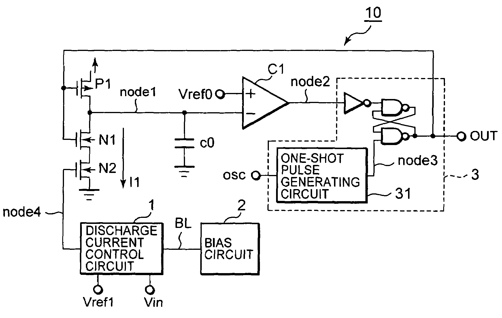
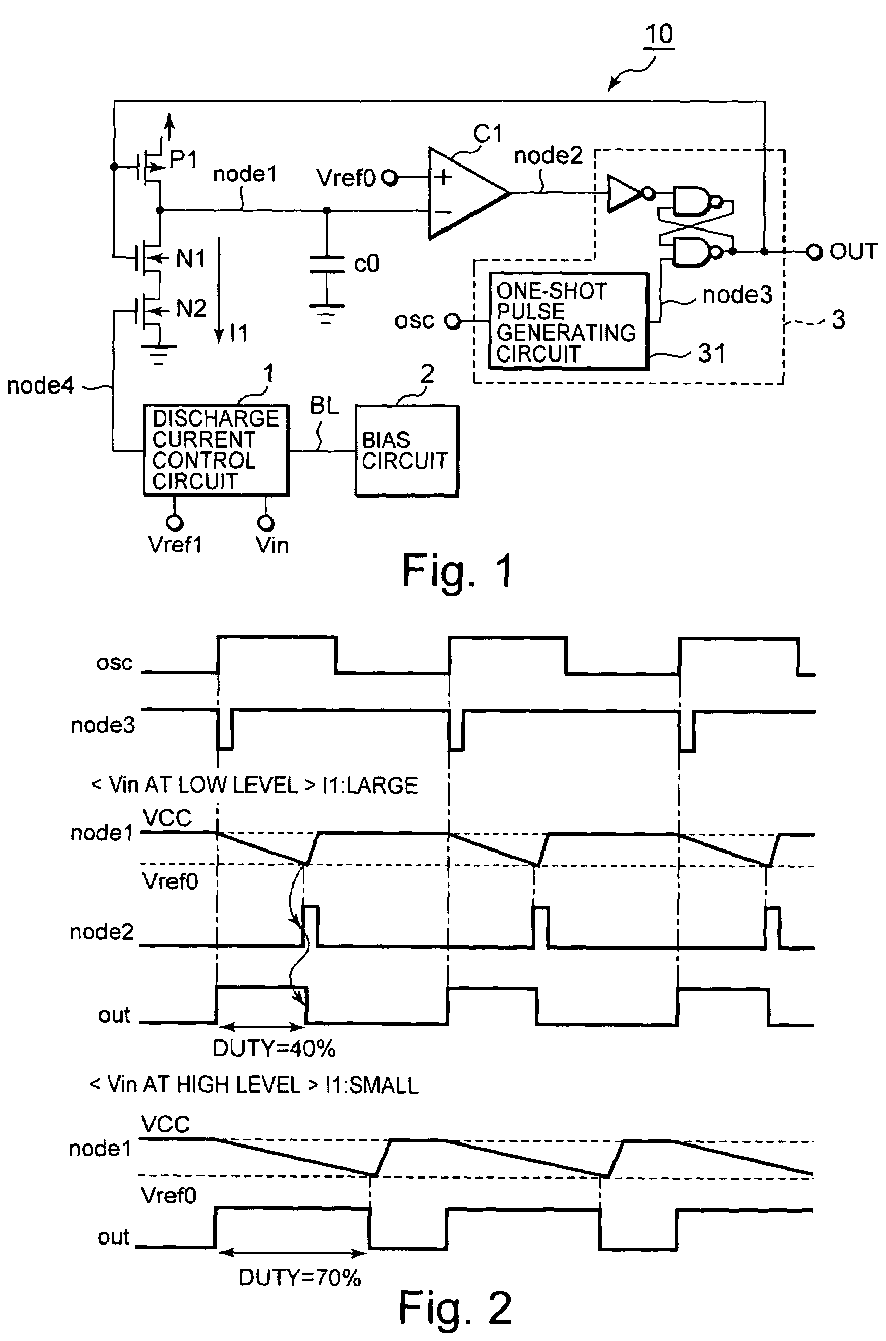
[0031]FIG. 1 is a diagram showing a configuration of a pulse width modulation (PWM) circuit according to a first embodiment of the present invention. The PWM circuit 10 is comprised of a PMOS transistor P1 for charging a node1, a NMOS transistor N1, N2 coupled serially to the PMOS transistor P1 for discharging stored charge on the node1 (an inverter comprised of a pair of the PMOS transistor P1 and the NMOS transistor N1 configures a charge and discharge means), a capacitor C0 coupled to the Node1, a comparator C1 that receives an input signal on the node1 and a reference signal Vref0, a discharge current control circuit that controls a fall-down time of a potential level of the node 1 by controlling a discharging current I1, a bias circuit 2 for generating a constant current and a PWM control circuit 3 that generates ON / OFF pulse signal for turning on and off the PMOS transistor P1 and the NMOS transistor N1 from a oscillator signal OSC and an output signal of the comparator C1 to ...

second preferred embodiment

[0050]FIG. 6 is a diagram showing a configuration of a PWM circuit according to a second embodiment of the present invention. The PWM circuit 20 is different as to comprising a NMOS transistor N3 coupled parallel to the NMOS transistor N2. The gate of the NMOS transistor N3 is coupled to the output BL of the bias circuit 2 and the drain is commonly coupled to the source of the NMOS transistor N1, and the source of it is coupled to the ground.

[0051]The operation of this PWM circuit will now be explained below. The basic operation of the circuit is similar to that of the first embodiment. In this embodiment, discharge current I1 is the sum of the current I3 of the NMOS transistor N3 and the current I2 of the NMOS transistor N2.

[0052]When a dimension ratio of the NMOS transistor N12 of the bias circuit 2 and that of the NMOS transistor N3 of the PWM circuit 20 is in a predetermined ratio (e.g. 1:n), the relation I3=n*If is satisfied (the If is a constant current of the NMOS transistor ...

third preferred embodiment

[0054]FIG. 7 is a diagram showing a configuration of a PWM circuit according to a third embodiment of the present invention. The PWM circuit 30 comprises a transfer gate 4 with PMOS transistor P1 and NMOS transistor N4 instead of the transistor P1 of the second preferred embodiment. The transfer gate 4 is controlled by the output signal OUT of the PWM control circuit 3. The circuit 30 also comprises an operational amplifier A1 which is configured as voltage follower with the input of reference voltage Vref2, the output of which is coupled to a terminal T1 of the transfer gate 4.

[0055]The operation of the PWM circuit 30 of the third preferred embodiment will now be described. The basic operation is similar to that of the first preferred embodiment, so only the difference of the operation will be described.

[0056]When the signal OSC is “low”, the transfer gate 4 is “on” and the node1 is charged up to the output level vref2 of the operational amplifier A1. The voltage level of Vref2 is ...


PUM


Abstract

The present invention provides a pulse width modulation (PWM) circuit comprising an PWM control circuit for setting an output signal to low when a logical level of a oscillation signal at a first input terminal changes from low to high, for resetting the output level to low in response to an effective input signal at a second terminal, a charge and discharge means for charging a first node (node1) when the output stays in low, for discharging the stored charge of node1 when the output stays in high, a comparator (C1) for outputting an output signal to the second terminal according to the first node signal and a first reference signal (Vref0), a discharge current controlling means for the stored charge on the first node, wherein the discharge current controlling means comprises a bias circuit 2 for controlling the discharge current based on constant current.

Description

BACKGROUND OF THE INVENTION[0001]The present invention relates to a pulse width modulation circuit (referred to below as PWM circuit) for modulating pulse width, more specially the invention relates to a PWM circuit that modulate pulse width at low frequency.[0002]FIG. 9 is a diagram showing an example of related PWM circuit. This circuit comprises a triangle wave generator with an input of oscillation signal (referred to below as OSC) and a comparator C1, the input of which is the output signal (node1) of the triangle wave generator (referred to below as TWG) and a signal Vin. FIG. 10 shows an example circuit of the TWG.[0003]The operation of the circuit of FIG. 9 is described below with reference to the FIG. 11. The TWG outputs a triangle wave signal on node1 according to the “high” and “low” level of input signal OSC. The comparator C1 compares the level of input signal Vin at non-inverting input terminal and the level of input signal of node1 at inverting input terminal, and out...

Claims


Application Information

Patent Timeline
Patent Type & Authority Patents(United States)
IPC IPC(8): H03K7/08H03K3/017H03K3/02H03K5/04
CPCG05B11/28C02F1/283C02F1/78C02F9/00C02F11/00
Inventor MATSUSHITA, YUICHI
Owner LAPIS SEMICON CO LTD
Why Eureka
Try Eureka