Substrate for producing a soldering connection

a technology of soldering connection and substrate, which is applied in the direction of soldering apparatus, manufacturing tools, printed circuit aspects, etc., can solve the problems of reducing the local stress maxima acting partially on individual balls, reducing the risk of short-circuiting bridges, and tearing of connections, so as to prevent the pad from peeling away from the substrate. , the effect of reducing the local stress maxima

Inactive Publication Date: 2007-09-18
POLARIS INNOVATIONS LTD
View PDF12 Cites 109 Cited by
  • Summary
  • Abstract
  • Description
  • Claims
  • Application Information

AI Technical Summary

Benefits of technology

[0017]In one aspect, the invention provides a substrate and a method for producing it which increases the reliability of soldering connections, particularly in the case of ball grid arrays having a high grid density by reducing in targeted fashion the risk of soldering connections tearing away on account of normal and shear stresses acting thereon.
[0032]Depending on the distribution of the solder balls on the substrate (ball-out) and the stress distribution essentially resulting therefrom over the entire ball-out, in accordance with further refinements according to the invention, the holding means are configured identically on all the soldering pads arranged for the electrical conduct-connection of a ball grid array or are distributed in such a way that their area-related weighting corresponds to the geometry and / or the direction of action of the mechanical loading acting on the entire soldering pad arrangement of a ball grid array. Particularly in the case of a spatially demanding and asymmetrical ball-out, local stress maxima acting partially on individual balls can be reduced by the holding means that are configured differently within the ball-out.

Problems solved by technology

If, moreover, different materials are also joined together by means of the soldering connection, a normal and shear loading acts on the soldering connections on account of the different coefficients of thermal expansion of the materials particularly on the part of a chip, which loading may lead to the connection tearing away.
As early as during the soldering process, a bulging of the substrates and components may occur, which may lead to a deformation of the balls in the z direction and also to latent stress states within the balls, thereby significantly impairing the reliability of individual soldering connections in the case where such local stress maxima occur simultaneously.
However, the increased amount of solder enhances the risk of the formation of short-circuiting bridges due to the solder repeatedly flowing out during the soldering process, since the required electrical spacings cannot be complied with, which may lead to electrical flashovers, or the solder ball electrically connects adjacent soldering pads to one another or to adjacent lines.
Application is usually effected by means of screen printing technology or phototechnology, screen printing being used less and less often because the fit tolerance that can be achieved with it is insufficient for many applications.
If the fit tolerance of the soldering resist mask is insufficient, the possible non-centric arrangement of soldering pad and resist-free region means that there is the risk of soldering bridge formation between the soldering pad and adjacent the conductor track, since the minimum electrical spacing between the soldering pad and the conductor track is not complied with or the solder even covers a part of the conductor track.
If a part of the soldering pad is covered by soldering resist on account of a non-centric arrangement or insufficient fit tolerance, a thin, transparent veil may arise on the soldering pad, the veil leading to soldering defects during soldering.
Consequently, during the subsequent production process, excessively narrow webs of the soldering resist mask can detach from the substrate and cause soldering bridges.
Such soldering pads with a soldering resist mask drawn back relatively far have a further soldering location defect which is typical of ball grid arrays and the cause of which resides in cracking at the interface of the substrate in the region below the soldering pad.
Under the mechanical loading described, the cracking practically leads to the peeling-away of the soldering pads including a superficial layer of the substrate and to the destruction of the line structure into which the soldering pad is integrated.
Therefore, if in the case of relatively dense ball grids and relatively dense line structures, the open resist-free regions of the soldering resist mask are made smaller than the soldering pads situated underneath, it is necessary to develop precise soldering resist edges since even a slight coverage of the soldering pad with soldering resist has the effect that a veil that forms covers the entire area and causes soldering defects.
Moreover, it has been ascertained that the peripheral sharp edge of the soldering resist exercises a notch effect on the soldering connection, thus resulting in a weakening of the connection and, even in the case of relatively low normal and shear stresses, the interruption of the soldering connection.
What is disadvantageous in this case, however, is that the production of this particular topography of the resist mask in the vicinity of the contact region requires particularly complex and cost-intensive methods and, depending on the method, possibly also additional transport and positioning sequences.
What is more, the improvement in the adhesion that can be achieved therewith is not sufficient for soldering connections with stress loadings such as occur in particular in the integration of BGA packages.
What is disadvantageous in this case, however, is that an enlargement of the soldering pads, on account of the ever-decreasing grid dimensions and the ever more demanding grid geometries, is appropriate either only in the edge region of the grid or in isolated fashion.

Method used


Image

  • Substrate for producing a soldering connection
  • Substrate for producing a soldering connection
  • Substrate for producing a soldering connection

Examples


Embodiment Construction

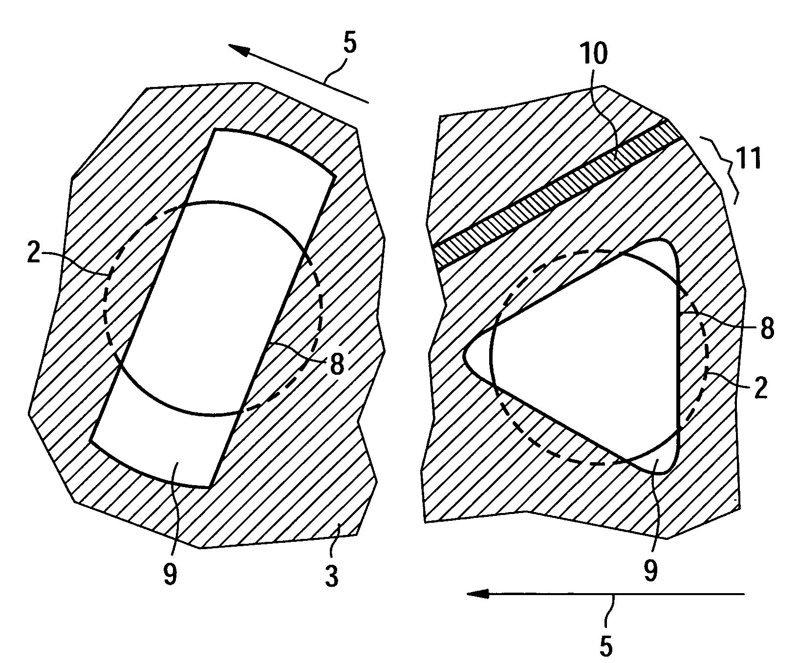
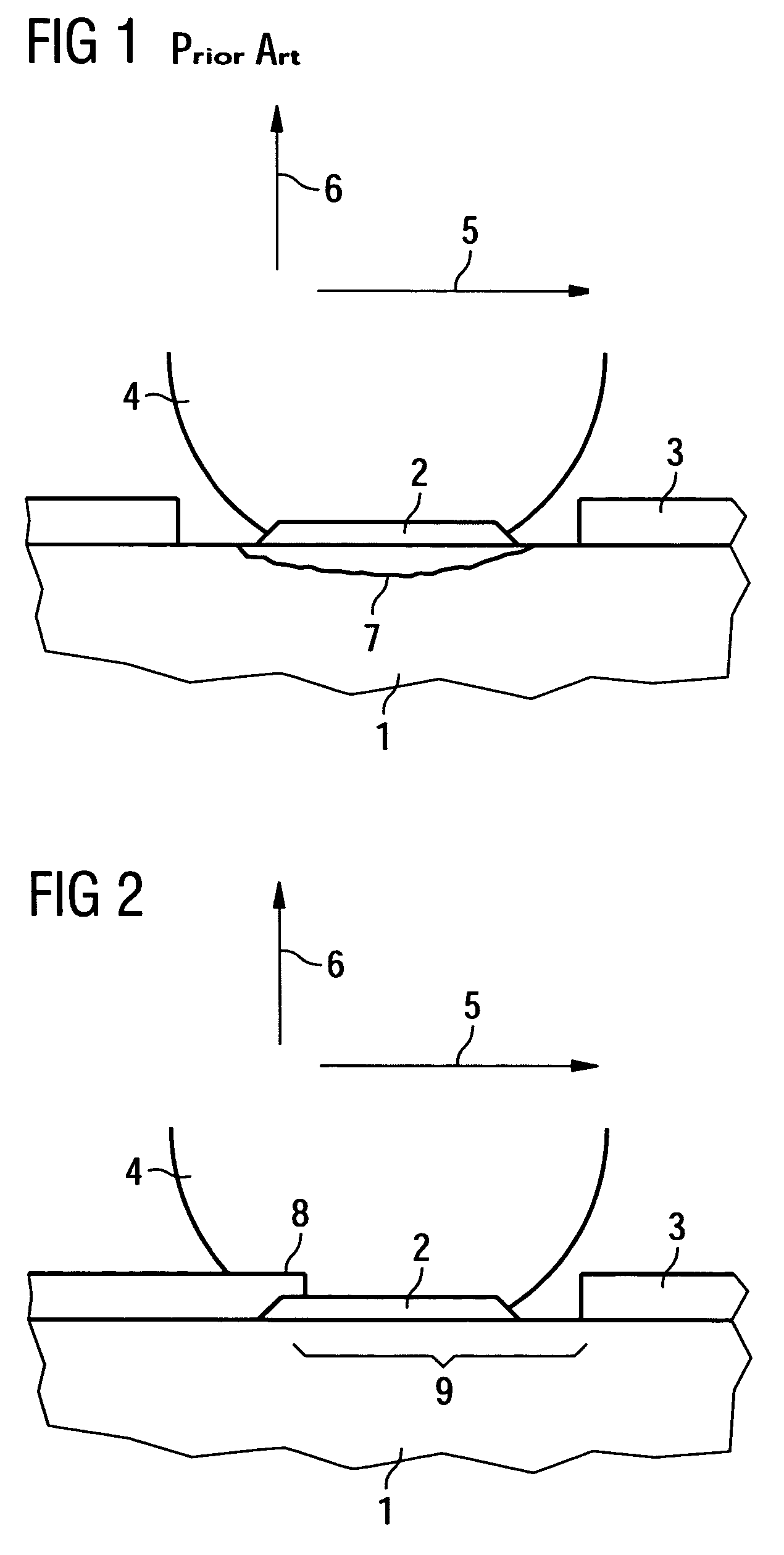
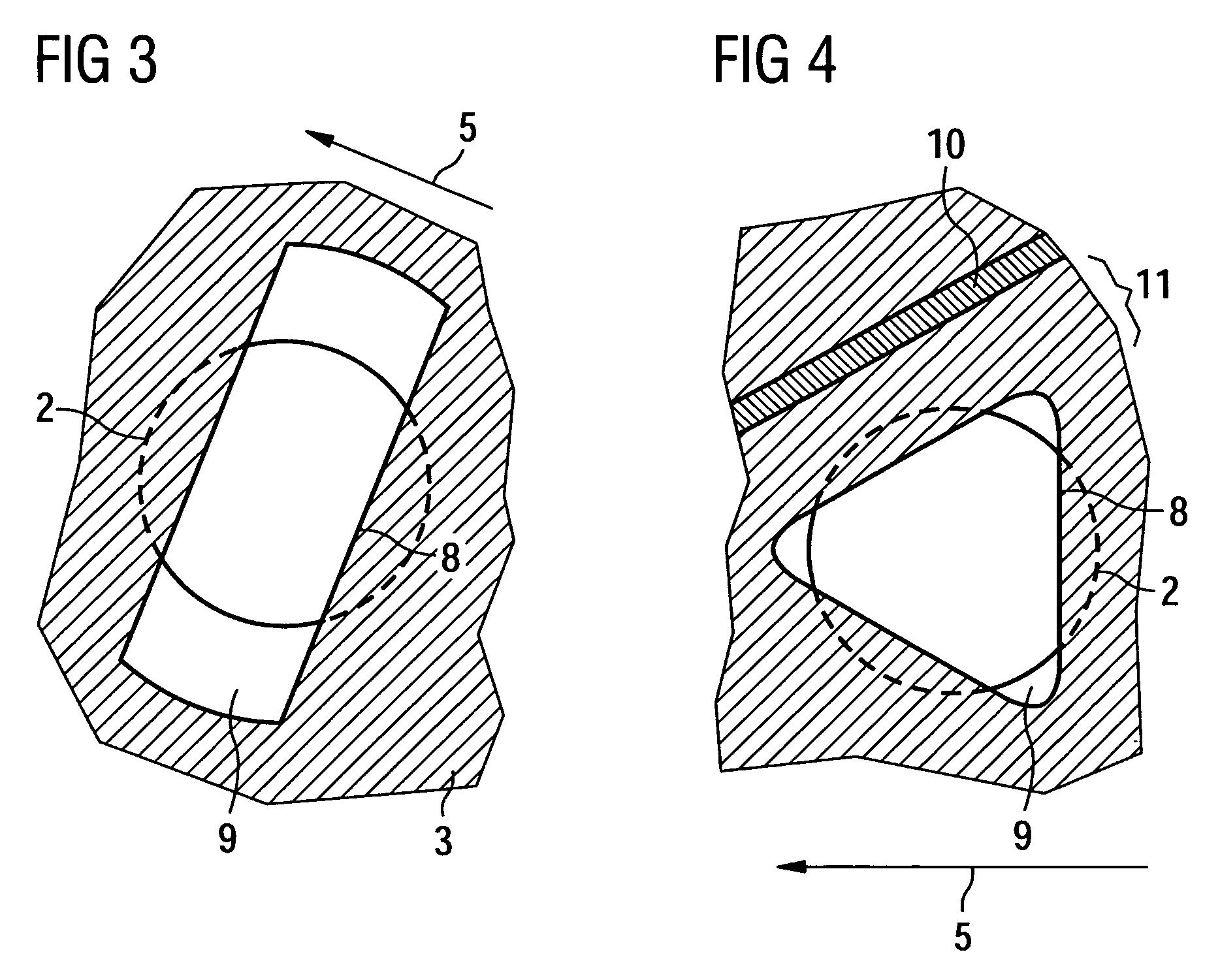
[0051]Embodiments of the present invention will now be described. In particular, a prior art configuration is shown in FIG. 1 while various aspects of the invention are described in FIGS. 2-4.

[0052]The soldering connection illustrated in FIG. 1, as corresponds to the prior art, has a substrate 1 with a soldering pad 2 arranged on its surface, the soldering pad is surrounded by a soldering resist mask 3. The soldering resist mask 3 is completely drawn back, so that the ball 4 of the solder is not in contact with the soldering resist mask 3. The laterally acting shear loading 5 illustrated and the perpendicularly acting normal loading 6 illustrated have led, in the present example, to the cracking 7 in the substrate surface and thus to the peeling-away of the soldering pad 2.

[0053]In accordance with the illustration in FIG. 2, assuming the same stress situation as in FIG. 1, due to shear loading 5 and normal loading 6, both of which are determined from the known test conditions of the...


PUM

PropertyMeasurementUnit
shapeaaaaaaaaaa
circular shapeaaaaaaaaaa
forceaaaaaaaaaa

Abstract

A solderable device includes a substrate and a soldering pad overlying the substrate. A solder mask overlies the substrate and portions of the soldering pad. The solder mask has an opening that exposes a portion of the soldering pad. The opening has at least two edges that symmetrically overlie portions of the soldering pad.

Description

[0001]This application claims priority to German Patent Application 103 44 390.8, which was filed Sep. 25, 2003, and to German Patent Application 10 2004 043 639.8, which was filed Sep. 7, 2004, both of which are incorporated herein by reference.TECHNICAL FIELD[0002]The present invention relates generally to soldering connections and more particularly to a substrate for producing a solder connection.BACKGROUND[0003]As is known, soldering connections that realize the electrical contact-connection of the semiconductor chips are exposed to particular mechanical stress input, particularly in the event of thermal cycling. If, moreover, different materials are also joined together by means of the soldering connection, a normal and shear loading acts on the soldering connections on account of the different coefficients of thermal expansion of the materials particularly on the part of a chip, which loading may lead to the connection tearing away. In this case, the tearing-away may take plac...

Claims


Application Information

Patent Timeline
Patent Type & Authority Patents(United States)
IPC IPC(8): H01L23/488B23K3/06H05K3/34
CPCB23K3/0638H05K3/3452H05K3/3457H05K2201/0989H05K2201/099
Inventor REISS, MARTINBENDER, CARSTENNOCKE, KERSTIN
Owner POLARIS INNOVATIONS LTD
Why Eureka
Try Eureka