Dual metal stud bumping for flip chip applications

a metal stud and flip chip technology, applied in the direction of soldering equipment, manufacturing tools, therapy, etc., can solve the problems of reducing the reliability of the formed package, deposited solder being exposed to high temperatures for extended periods of time, uneven height of the resulting solder ball on the semiconductor die,

Inactive Publication Date: 2007-09-18
SEMICON COMPONENTS IND LLC
View PDF43 Cites 114 Cited by
  • Summary
  • Abstract
  • Description
  • Claims
  • Application Information

AI Technical Summary

Problems solved by technology

Because of the deformation, the heights of the resulting solder balls on the semiconductor die can be uneven.
If this happens, the strength of the formed solder joints may be weak thus potentially decreasing the reliability of the formed package.
Moreover, during the reflow process, the deposited solder is exposed to high temperatures for extended periods of time.
Excessively heating the deposited solder can promote excessive intermetallic growth in the solder deposits.
Intermetallics in the solder joints make the solder joints brittle and reduce the fatigue resistance of the solder joints.
Lastly, performing a full reflow process takes time and energy and thus adds to the cost of the die package that is finally produced.
While the described stud bumping approach is feasible, there are some problems to be addressed.
Second, voids can form between the copper in the copper stud and the thick intermetallic compound layer.
The gap results in a poor electrical and mechanical connection between the semiconductor die and the carrier to which it is attached.

Method used


Image

  • Dual metal stud bumping for flip chip applications
  • Dual metal stud bumping for flip chip applications
  • Dual metal stud bumping for flip chip applications

Examples


Embodiment Construction

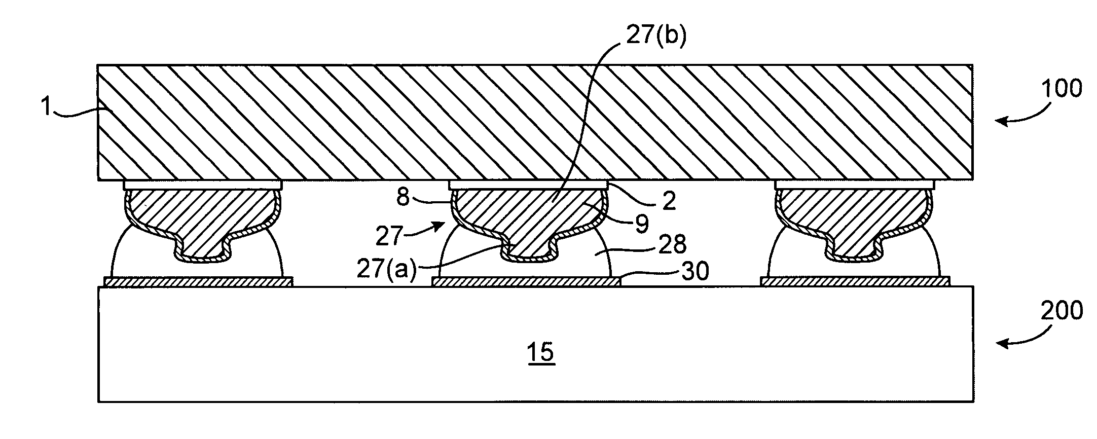
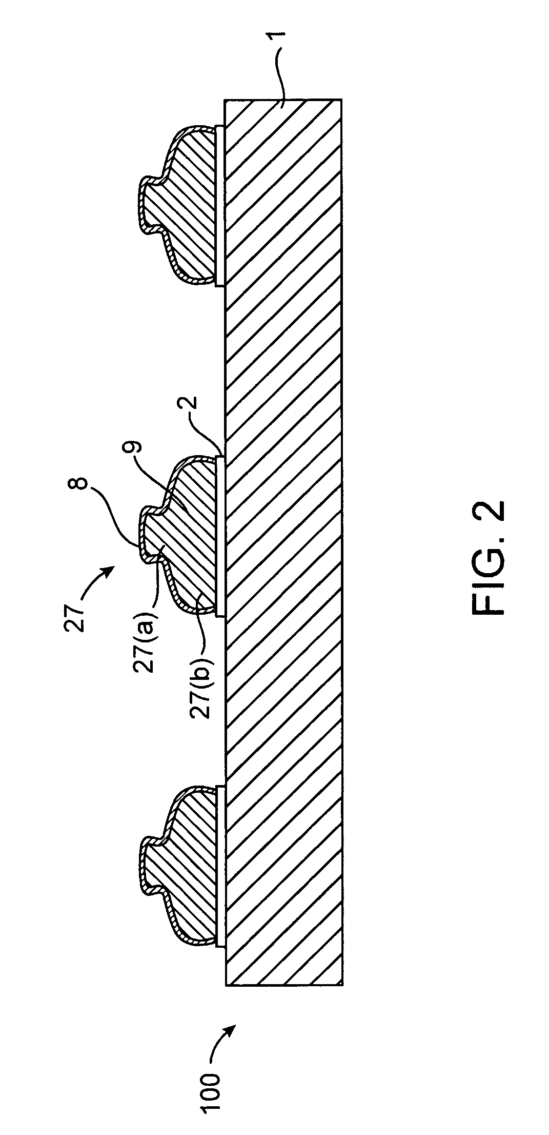
[0019]FIG. 2 shows a stud bumped semiconductor die 100 according to an embodiment of the invention. The stud bumped semiconductor die 100 has a semiconductor die 1 including first conductive regions 2, and conductive stud bumps 27 on the first conductive regions 2.

[0020]The semiconductor die 100 may comprise any suitable material (e.g., silicon, gallium arsenide) and may include any suitable active or passive semiconductor device. For example, the semiconductor die may comprise a metal oxide field effect transistor (MOSFET) such as a power MOSFET. The MOSFET may have a planar or trenched gate. Trenched gates are preferred. Transistor cells containing trenched gates are narrower than planar gates. In addition, the MOSFET may be a vertical MOSFET. In a vertical MOSFET, the source region and the drain region are at opposite sides of the semiconductor die so that current in the transistor flows vertically through the semiconductor die.

[0021]Each conductive region 2 may be, for example, ...


PUM

PropertyMeasurementUnit
thicknessaaaaaaaaaa
diameteraaaaaaaaaa
oxidation resistantaaaaaaaaaa

Abstract

A method for forming a stud bumped semiconductor die is disclosed. The method includes forming a ball at the tip of a coated wire passing through a hole in a capillary, where the coated wire has a core and an oxidation-resistant coating. The formed ball is pressed to the conductive region on the semiconductor die. The coated wire is cut, thereby leaving a conductive stud bump on the conductive region, where the conductive stud bump includes an inner conductive portion and an outer oxidation-resistant layer.

Description

BACKGROUND OF THE INVENTION[0001]There are many different levels of packages and interconnections in electronic packages. In a typical first level packaging process, a silicon die is joined to a ceramic substrate carrier. In a typical second level packaging process, the ceramic substrate carrier with the die is mounted on an organic board.[0002]In one conventional method for forming a first level package, a passivation layer is formed on a semiconductor die (which may be in a semiconductor wafer). The passivation layer includes apertures that expose conductive regions on the semiconductor die. Titanium and copper layers are sputtered on the upper surface of the conductive regions and the passivation layer. A layer of photoresist is then patterned on the semiconductor die so that the apertures in the patterned photoresist layer are over the conductive regions. Solder is electroplated in the apertures in the photoresist layer until the apertures are filled with solder. The photoresist...

Claims


Application Information

Patent Timeline
Patent Type & Authority Patents(United States)
IPC IPC(8): H01L23/52H01L23/48H01L29/40H01L21/60H01L23/485
CPCH01L24/11H01L24/16H01L24/81H01L24/13H01L2924/1306H01L2924/10253H01L2224/81193H01L2924/00013H01L2224/81192H01L2224/1134H01L2224/13099H01L2224/13111H01L2224/13147H01L2224/16H01L2224/81801H01L2924/01013H01L2924/01022H01L2924/01029H01L2924/01033H01L2924/01046H01L2924/01047H01L2924/01051H01L2924/01078H01L2924/01079H01L2924/01082H01L2924/01327H01L2924/10329H01L2924/13091H01L2924/19043H01L2924/01005H01L2924/01006H01L2924/01024H01L2924/0105H01L2924/014H01L2224/29099H01L2924/00H01L2924/15787H01L2924/181H01L2224/05573H01L2224/05568A61N1/395A61N1/3956H01L2224/11H01L2224/05655H01L2924/00014H01L2224/05666H01L2224/05124
Inventor JOSHI, RAJEEVTANGPUZ, CONSUELORIOS, MARGIE T.CRUZ, ERWIN VICTOR R.
Owner SEMICON COMPONENTS IND LLC
Why Eureka
Try Eureka