Electroluminescent display device, method for manufacturing the same, and electronic equipment

a technology of electroluminescent display device and manufacturing method, which is applied in the direction of discharge tube/lamp details, discharge tube luminescnet screen, organic semiconductor device, etc., can solve the problems of reduced product life, reduced pixel aperture ratio, and degraded luminescent characteristics, and achieve high luminous efficacy

Inactive Publication Date: 2007-09-18
SEIKO EPSON CORP
View PDF20 Cites 19 Cited by
  • Summary
  • Abstract
  • Description
  • Claims
  • Application Information

AI Technical Summary

Benefits of technology

[0012]In the present configuration, the average oxygen concentration in the second electrode is controlled to become at least a predetermined concentration in order to attain transparency required for display, and there is a concentration gradient in the film thickness direction. For example, the oxygen concentration in the lower portion (toward the function layer) is lower than the oxygen concentration in the upper layer side, and the oxygen concentration in the vicinity of the interface with the function layer is lower than the above-described predetermined concentration. Consequently, when the above-described metal oxide film is deposited by sputtering in the vicinity of the interface with the function layer, the partial pressure of oxygen in the carrier gas can be lowered more than in prior arts and, therefore, oxidation of the function layer serving as a substrate can be minimized during the film formation. In this manner, reduction in luminous efficacy of the function layer can be reduced or prevented, and bright display can be realized. In particular, desirably, the oxygen concentration in the vicinity of the interface with the function layer is substantially zero and, thereby, damage to the function layer due to oxidation during the film formation can be minimized.
[0016]In the present manufacturing method, when the metal oxide film is deposited by sputtering on the function layer, the partial pressure of oxygen in the initial stage of the film formation can be lowered more than in the related art. Therefore, oxidation of the function layer due to active oxygen in the carrier gas can be minimized, and a display device having a high luminous efficacy can be prepared. Since the partial pressure of oxygen in the carrier gas is increased with increased deposition of the metal oxide film, the transparency of the whole second electrode required for display can be attained by increasing the oxygen concentration in the upper layer side in order that the oxygen concentration in second electrode as a whole becomes at least the above-described predetermined concentration.
[0017]When the partial pressure of oxygen in the above-described carrier gas is increased during the above-described sputtering, preferably, the partial pressure of oxygen is increased continuously or stepwise. In this manner, a desired average oxygen concentration suitable to attain the transparency required for display can easily be attained.
[0018]Since the partial pressure of oxygen in the carrier gas is controlled to be substantially zero when the above-described amount of deposition is less than a predetermined film thickness during the above-described sputtering, oxidation of the function layer can be completely reduced or prevented.
[0021]According to the present configuration, the electronic equipment including a display portion having a high luminous efficacy can be provided.

Problems solved by technology

However, the upsizing of the above-described bottom emission type EL display device requires a thick wiring to supply signals to electrodes and, thereby, a problem of reduction in aperture ratio of the pixel occurs.
When the aperture ratio is reduced as described above, a large current is passed through the luminescent layer in order to ensure the brightness of the pixel and, as a result, a problem of a reduction in the product life occurs as well.
However, in the formation of the metal oxide by sputtering on the EL layer or an electron injection layer (or a hole injection layer) provided on the EL layer, there is a problem in that the substrate EL layer may be oxidized by active oxygen in the carrier gas and, thereby, the luminescent characteristics are degraded.

Method used


Image

  • Electroluminescent display device, method for manufacturing the same, and electronic equipment
  • Electroluminescent display device, method for manufacturing the same, and electronic equipment
  • Electroluminescent display device, method for manufacturing the same, and electronic equipment

Examples


first exemplary embodiment

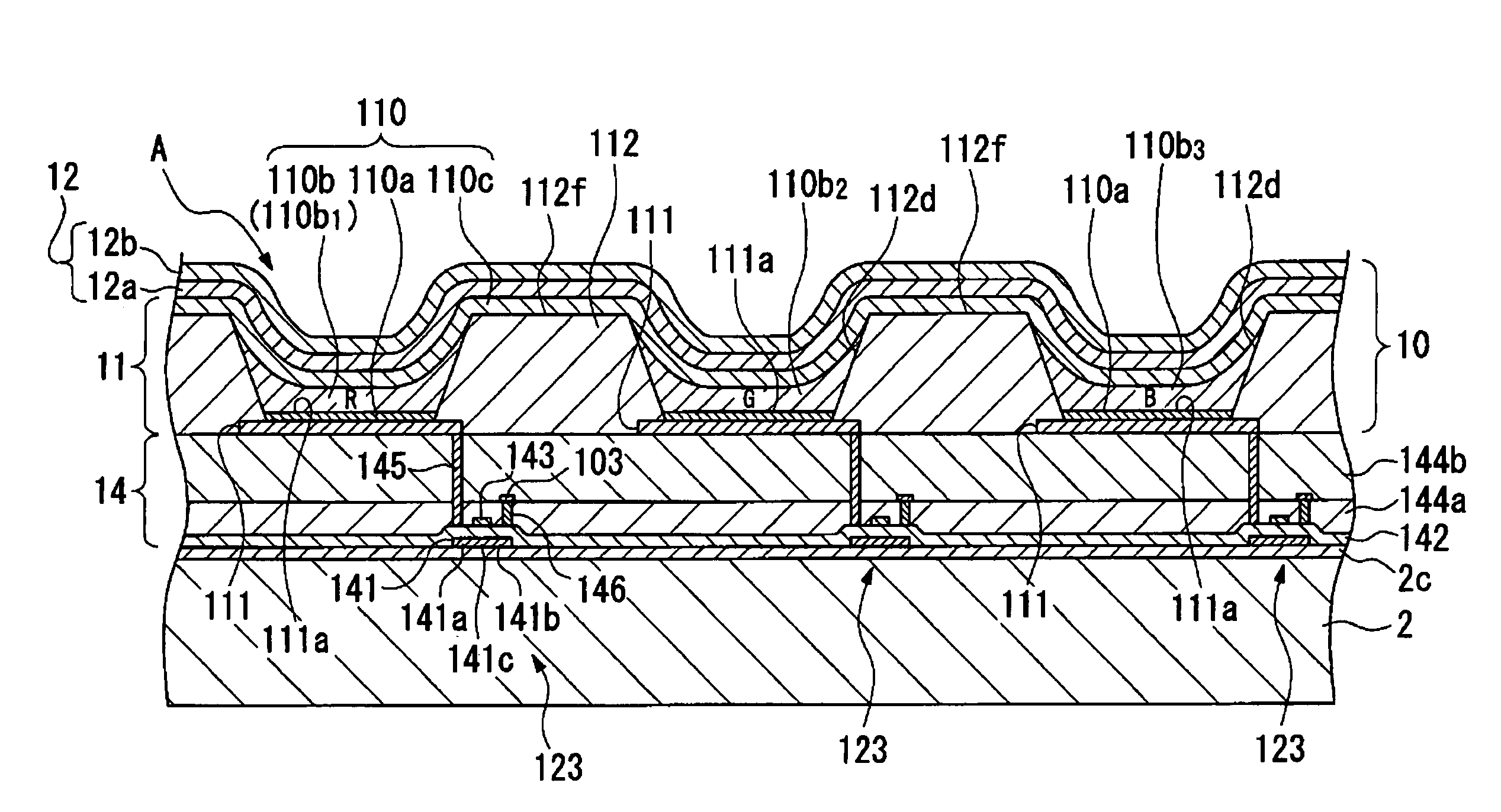
[0045]The first exemplary embodiment of the present invention will be described below with reference to the figures. In FIG. 1 to FIG. 18, the scale of each layer or each element is differentiated from each other in order that each layer or each element has a size capable of being identified in the figure.

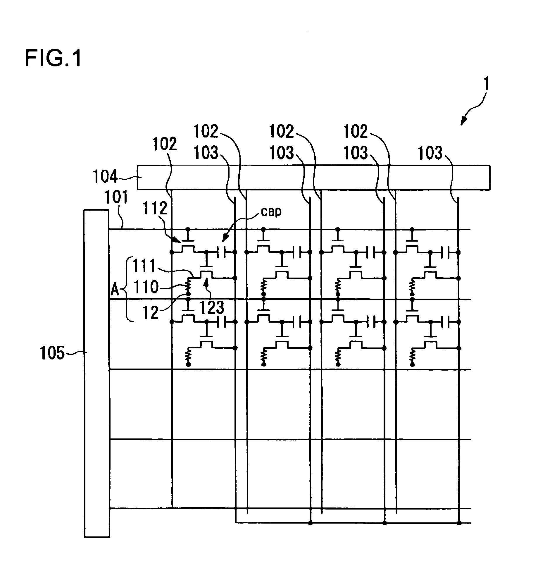
[0046]FIG. 1 is a schematic plan view showing the wiring structure of an organic EL display device as an example of an electroluminescent display device according to the present exemplary embodiment.

[0047]As shown in FIG. 1, the electroluminescent display device 1 of the present exemplary embodiment is provided with wirings of a plurality of scanning lines 101, a plurality of signal lines 102 extending in the direction intersecting the scanning lines 101, and a plurality of power source lines 103 extending parallel to the signal lines 102. Regions separated by the scanning lines and the signal lines are configured as pixel regions.

[0048]The signal lines are connected to a data-side...

second exemplary embodiment

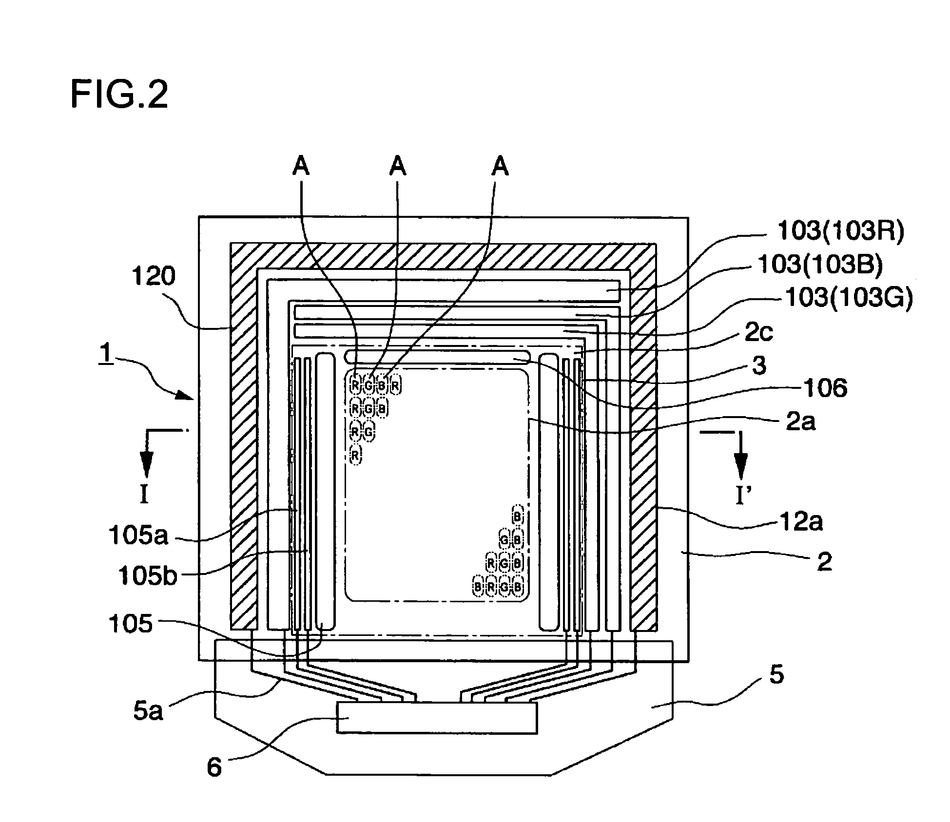
[0172]The second exemplary embodiment of the present invention will be described with reference to FIG. 21. In the following description, portions similar to those in the above-described first exemplary embodiment are indicted by the same reference numerals as in the first exemplary embodiment, and a part of explanations thereof will not be provided. The description will be made with reference to FIG. 2 and FIG. 3 as appropriate.

[0173]An electroluminescent display device of the present exemplary embodiment is configured as an EL display device having a so-called reverse structure in which cathodes 111′, electron injection layers 110a′, luminescent layers 110b, a hole injection / transportation layer 110c′, and an anode 12′ are laminated in that order from the substrate 2 side. In the present display device, a function layer 110′ is composed of the electron injection layer 110a′, the luminescent layer 110b, and the hole injection / transportation layer 110c′.

[0174]The present display de...


PUM

PropertyMeasurementUnit
thicknessaaaaaaaaaa
thicknessaaaaaaaaaa
thicknessaaaaaaaaaa

Abstract

A transparent cathode electrode technology for an electroluminescent display device having a top emission structure, provides a top emission type electroluminescent display device and a method to manufacture the same. Oxidation of a substrate film can be reduced or prevented during the film formation of a metal oxide. Electronic equipment including this display device is also provided. A first electrode, a function layer including a luminescent layer, and a transparent second electrode made of a metal oxide are laminated on the substrate in that order from the lower surface. At this time, the oxygen concentration in the second electrode is made to vary in the film thickness direction, and the oxygen concentration in the vicinity of the interface between the second electrode and the function layer is made lower than the average oxygen concentration in the second electrode.

Description

BACKGROUND OF THE INVENTION[0001]1. Field of Invention[0002]The present invention relates to an electroluminescent display device, a method to manufacture the same, and electronic equipment provided with this electroluminescent display device.[0003]2. Description of Related Art[0004]Electroluminescent (hereafter referred to as EL) display devices have been developed until now as display device for portable devices, e.g., cellular phones and PDAs, personal computers, and the like.[0005]The EL display device is configured to include a plurality of luminescent elements, which is composed of a pair of electrodes holding an EL layer (electroluminescent layer) therebetween, in a substrate surface, and desired display is performed by independently controlling the driving of each luminescent element. This EL display device can be classified into, for example, a bottom emission type which takes light from the side of the element substrate and a top emission type which takes light from the si...

Claims


Application Information

Patent Timeline
Patent Type & Authority Patents(United States)
IPC IPC(8): H01L51/00H05B33/28C23C14/08C23C14/34H01B13/00H01L27/32H01L51/30H01L51/50H01L51/52H05B33/10H05B33/14H05B33/26
CPCH01L51/5234H01L27/3244H01L51/0036H01L51/0038H01L2251/5315H01L51/0043H01L51/0059H01L51/0039H10K59/12H10K85/115H10K85/114H10K85/113H10K85/151H10K85/631H10K50/828H10K2102/3026H05B33/26
Inventor KOBAYASHI, HIDEKAZU
Owner SEIKO EPSON CORP
Why Eureka
Try Eureka