Electroluminescent display device, method for manufacturing the same, and electronic equipment

Inactive Publication Date: 2005-02-24
SEIKO EPSON CORP
View PDF5 Cites 18 Cited by
  • Summary
  • Abstract
  • Description
  • Claims
  • Application Information

AI Technical Summary

Benefits of technology

[0021] According to the present configuration, the electronic equipment in

Problems solved by technology

However, the upsizing of the above-described bottom emission type EL display device requires a thick wiring to supply signals to electrodes and, thereby, a problem of reduction in aperture ratio of the pixel occurs.
When the aperture ratio is reduced as described above, a large current is passed through the luminescent layer in order to ensure the brightness of the pixel and, as a res

Method used


Image

  • Electroluminescent display device, method for manufacturing the same, and electronic equipment
  • Electroluminescent display device, method for manufacturing the same, and electronic equipment
  • Electroluminescent display device, method for manufacturing the same, and electronic equipment

Examples


first exemplary embodiment

[0045] First Exemplary Embodiment

[0046] The first exemplary embodiment of the present invention will be described below with reference to the figures. In FIG. 1 to FIG. 18, the scale of each layer or each element is differentiated from each other in order that each layer or each element has a size capable of being identified in the figure.

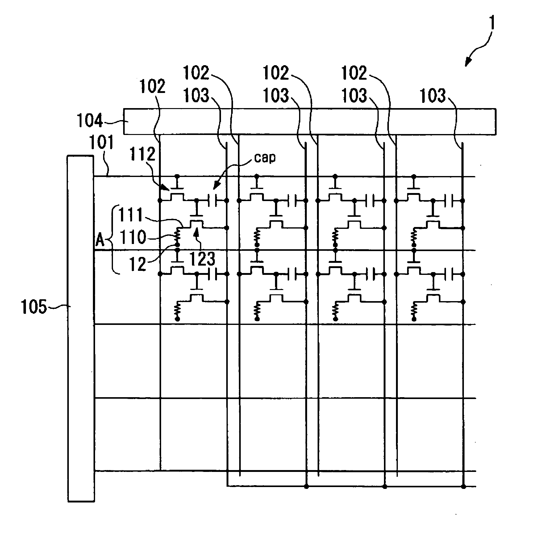
[0047]FIG. 1 is a schematic plan view showing the wiring structure of an organic EL display device as an example of an electroluminescent display device according to the present exemplary embodiment.

[0048] As shown in FIG. 1, the electroluminescent display device 1 of the present exemplary embodiment is provided with wirings of a plurality of scanning lines 101, a plurality of signal lines 102 extending in the direction intersecting the scanning lines 101, and a plurality of power source lines 103 extending parallel to the signal lines 102. Regions separated by the scanning lines and the signal lines are configured as pixel regions.

[0049] The si...

second exemplary embodiment

[0183] Second Exemplary Embodiment

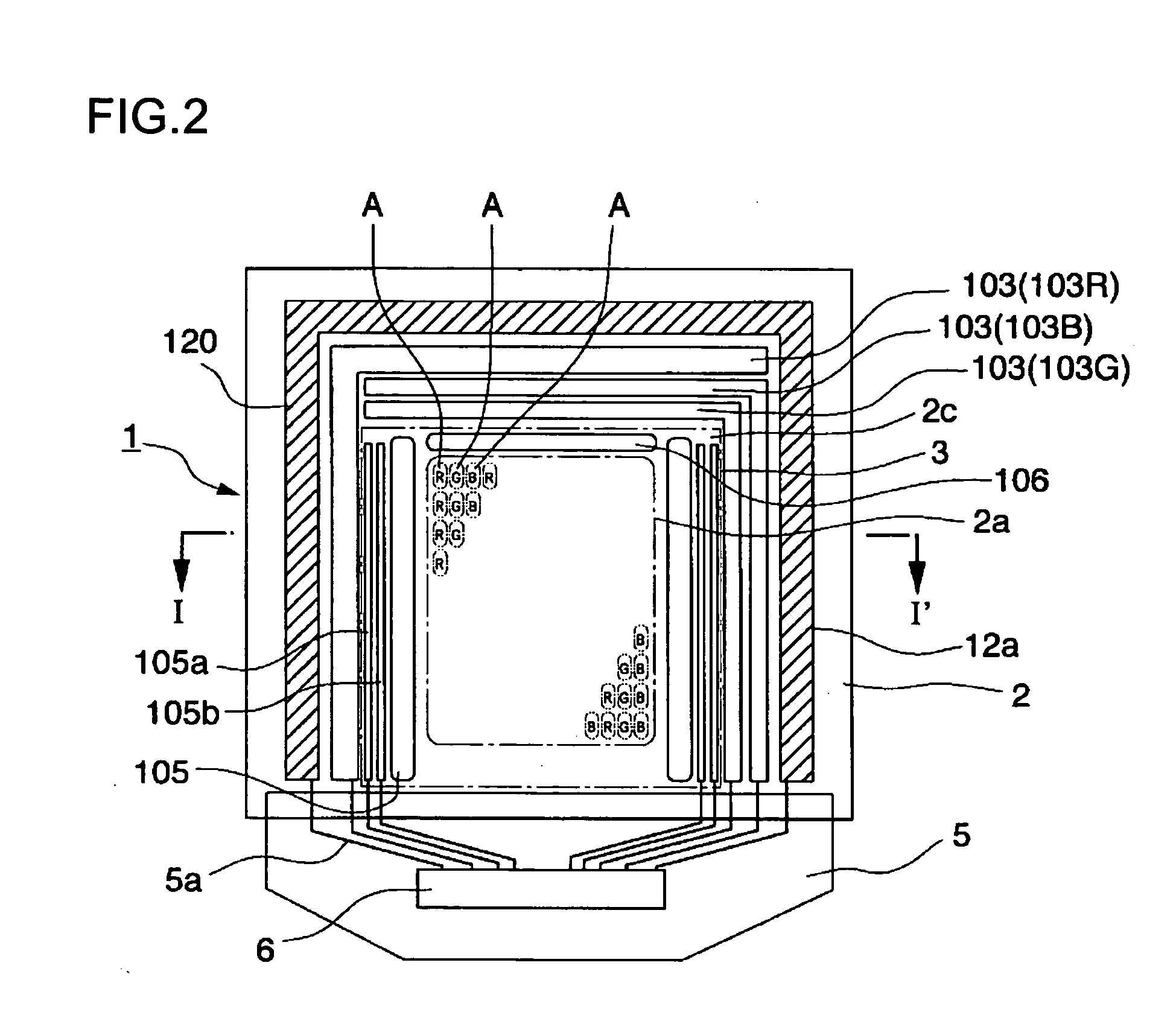
[0184] The second exemplary embodiment of the present invention will be described with reference to FIG. 21. In the following description, portions similar to those in the above-described first exemplary embodiment are indicted by the same reference numerals as in the first exemplary embodiment, and a part of explanations thereof will not be provided. The description will be made with reference to FIG. 2 and FIG. 3 as appropriate.

[0185] An electroluminescent display device of the present exemplary embodiment is configured as an EL display device having a so-called reverse structure in which cathodes 111′, electron injection layers 110a′, luminescent layers 110b, a hole injection / transportation layer 110c′, and an anode 12′ are laminated in that order from the substrate 2 side. In the present display device, a function layer 110′ is composed of the electron injection layer 110a′, the luminescent layer 110b, and the hole injection / transportation laye...


PUM

PropertyMeasurementUnit
Thicknessaaaaaaaaaa
Thicknessaaaaaaaaaa
Thicknessaaaaaaaaaa

Abstract

A transparent cathode electrode technology for an electroluminescent display device having a top emission structure, provides a top emission type electroluminescent display device and a method to manufacture the same. Oxidation of a substrate film can be reduced or prevented during the film formation of a metal oxide. Electronic equipment including this display device is also provided. A first electrode, a function layer including a luminescent layer, and a transparent second electrode made of a metal oxide are laminated on the substrate in that order from the lower surface. At this time, the oxygen concentration in the second electrode is made to vary in the film thickness direction, and the oxygen concentration in the vicinity of the interface between the second electrode and the function layer is made lower than the average oxygen concentration in the second electrode.

Description

BACKGROUND OF THE INVENTION [0001] 1. Field of Invention [0002] The present invention relates to an electroluminescent display device, a method to manufacture the same, and electronic equipment provided with this electroluminescent display device. [0003] 2. Description of Related Art [0004] Electroluminescent (hereafter referred to as EL) display devices have been developed until now as display device for portable devices, e.g., cellular phones and PDAs, personal computers, and the like. [0005] The EL display device is configured to include a plurality of luminescent elements, which is composed of a pair of electrodes holding an EL layer (electroluminescent layer) therebetween, in a substrate surface, and desired display is performed by independently controlling the driving of each luminescent element. This EL display device can be classified into, for example, a bottom emission type which takes light from the side of the element substrate and a top emission type which takes light f...

Claims


Application Information

Patent Timeline
IPC IPC(8): C23C14/08H05B33/28C23C14/34H01B13/00H01L27/32H01L51/00H01L51/30H01L51/50H01L51/52H05B33/10H05B33/14H05B33/26
CPCH01L27/3244H01L51/0036H01L51/0038H01L2251/5315H01L51/0043H01L51/0059H01L51/5234H01L51/0039H10K59/12H10K85/115H10K85/114H10K85/113H10K85/151H10K85/631H10K50/828H10K2102/3026H05B33/26
Inventor KOBAYASHI, HIDEKAZU
Owner SEIKO EPSON CORP
Why Eureka
Try Eureka