Method and circuit using boundary scan cells for design library analysis

a technology of design library and scan cell, applied in error detection/correction, program control, instruments, etc., can solve the problems of low design improvement potential, and low design improvement potential, and achieve the effect of improving design feasibility, reducing test chip cost, and improving design feasibility

Active Publication Date: 2007-10-09
GOOGLE LLC
View PDF17 Cites 6 Cited by
  • Summary
  • Abstract
  • Description
  • Claims
  • Application Information

AI Technical Summary

Problems solved by technology

In limited volume production such as that found in the application specific integrated circuit (ASIC) realm, potential design improvements are difficult to assess because of the low volumes.
While there are many techniques for testing integrated chips, current testing methodology provides little information useful to the designer of integrated circuits in terms of determining the effects of different process technology device library elements or different latch circuit implementations on integrated circuit performance.
However test chips are expensive to design and fabricate and cannot normally be run in sufficient volume in limited volume production scenarios such as found in the ASIC realm.

Method used


Image

  • Method and circuit using boundary scan cells for design library analysis
  • Method and circuit using boundary scan cells for design library analysis
  • Method and circuit using boundary scan cells for design library analysis

Examples


Embodiment Construction

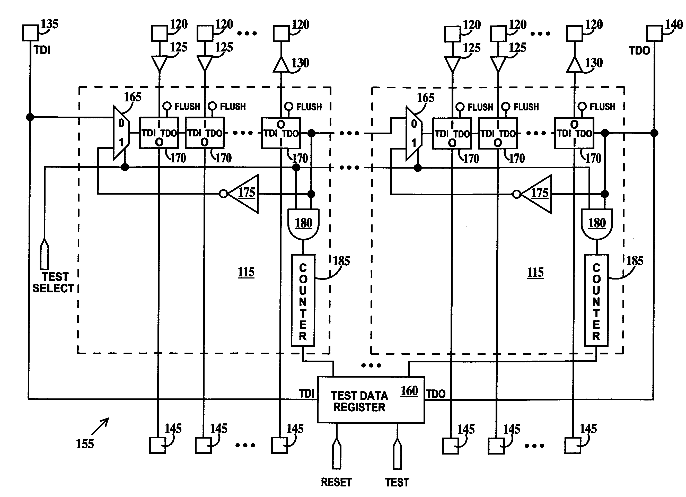
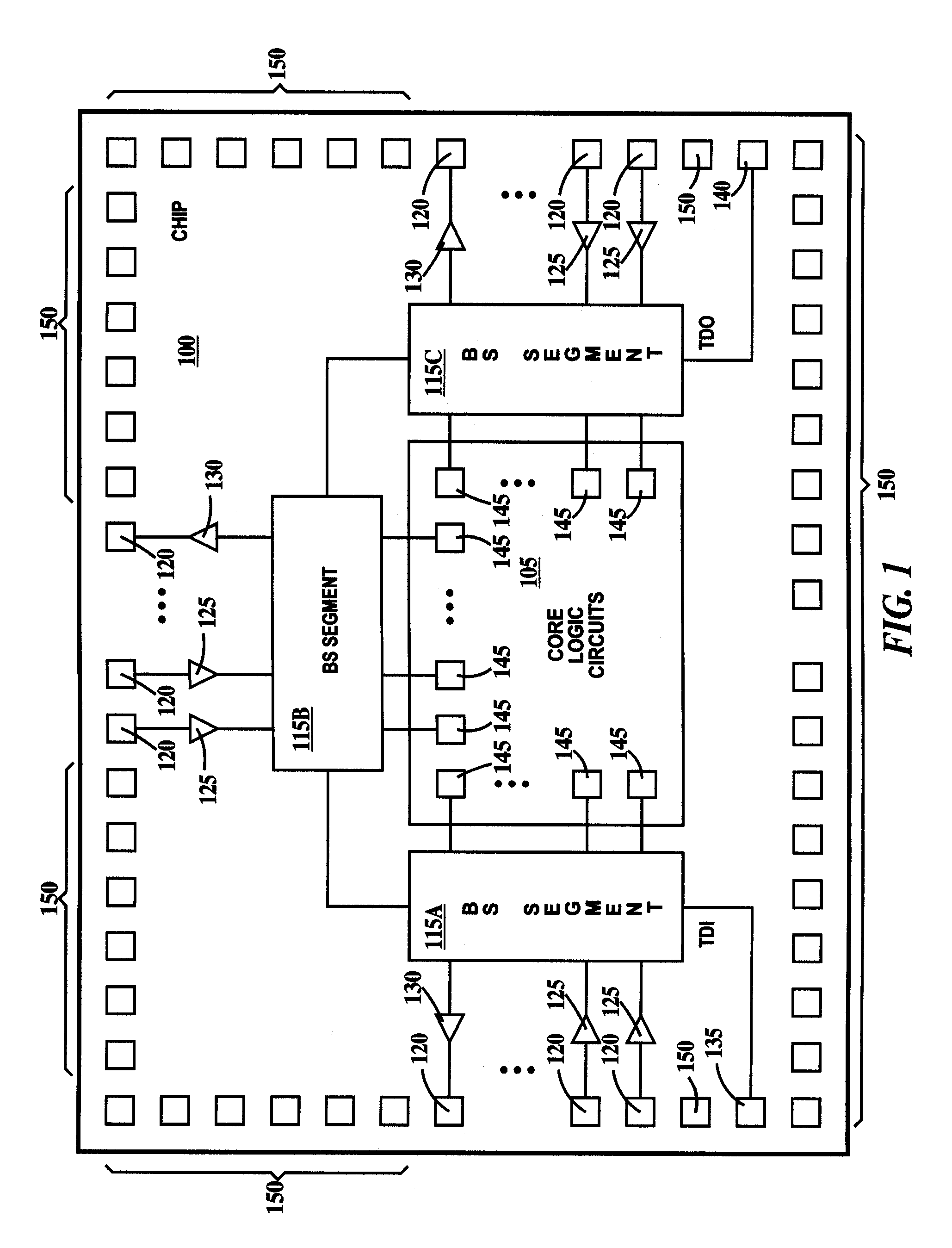
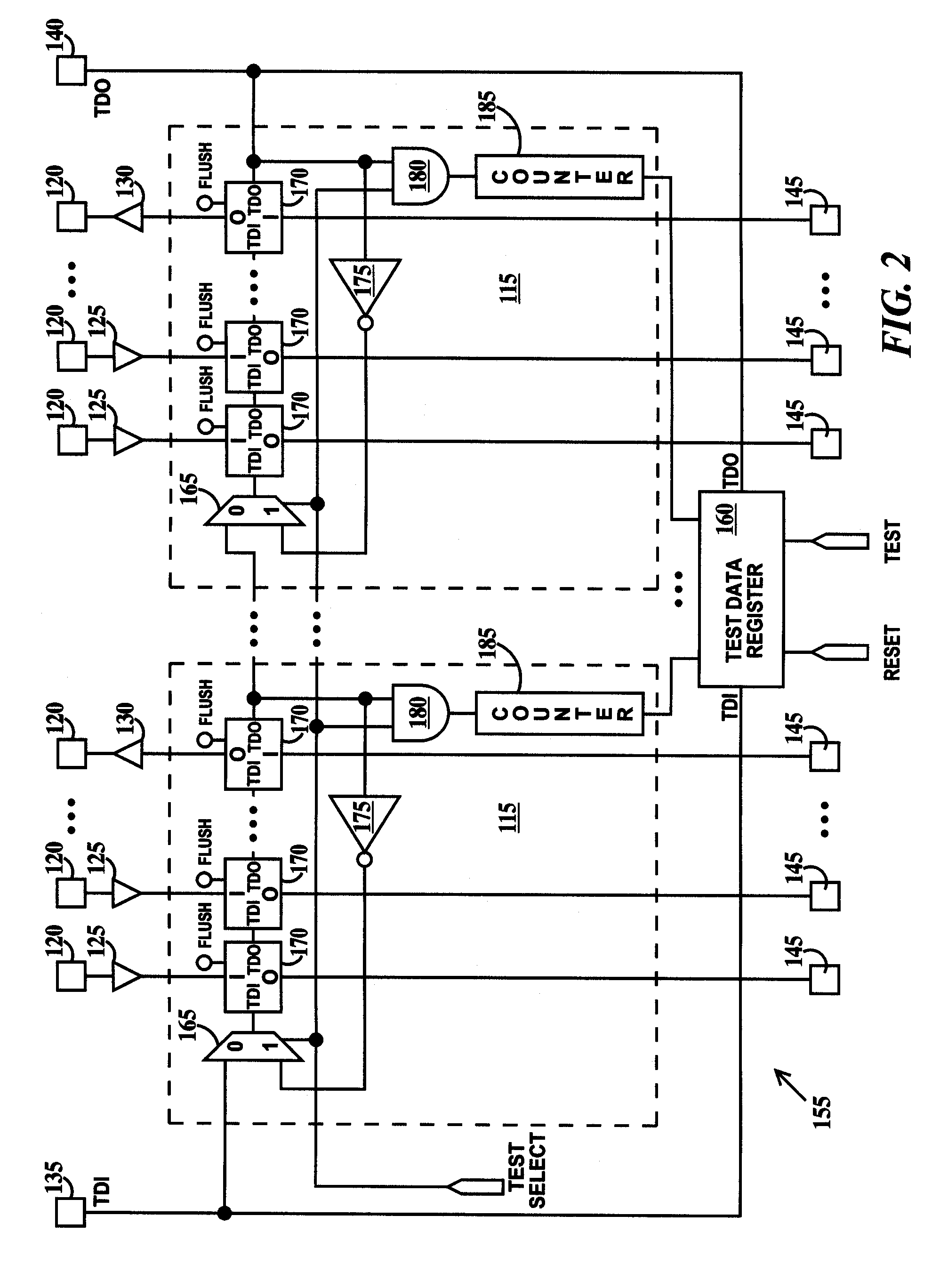
[0015]References to IEEE 1149.1 standards are to the Institute of Electrical and Electronic Engineers) IEEE standard 1149.1 which is defined by the Standard Test Access Port and Boundary Scan Architecture, Institute of Electrical and Electronics Engineers (May 21, 1990) and the 1149.1b-1994 Supplement.

[0016]For the purposes of the present invention a flip-flop is a type of latch, a pad is a physical chip structure for connecting the integrated circuit chip to the outside world and a pin is an internal chip connection point between circuits within an integrated circuit chip. The terms nominal design threshold voltage, nominal gate dielectric thickness and nominal channel length indicates a voltage, thickness or length specified for a device from a particular process technology library to meet a pre-determined device (i.e. transistor) performance specification. A latch circuit implementation is a function of the selection and interconnection of transistors, logic gates and other circu...


PUM


Abstract

A boundary scan register circuit and a method of characterization testing. The boundary scan register circuit, including: a multiplicity of boundary scan cells connected in series, each boundary scan cell having a latch; means for isolating the boundary scan cells into one or more boundary scan segments, each boundary scan segment containing a different set of the boundary scan cells; and means for characterizing signal propagation through each boundary scan segment.

Description

FIELD OF THE INVENTION[0001]The present invention relates to the field of boundary scan testing; more specifically, it relates to a method and circuit characterization of process technology libraries and circuit implementations of latches using boundary scan registers.BACKGROUND OF THE INVENTION[0002]In limited volume production such as that found in the application specific integrated circuit (ASIC) realm, potential design improvements are difficult to assess because of the low volumes. While there are many techniques for testing integrated chips, current testing methodology provides little information useful to the designer of integrated circuits in terms of determining the effects of different process technology device library elements or different latch circuit implementations on integrated circuit performance. Evaluations can be performed using test chips. However test chips are expensive to design and fabricate and cannot normally be run in sufficient volume in limited volume ...

Claims


Application Information

Patent Timeline
Patent Type & Authority Patents(United States)
IPC IPC(8): G01R31/28
CPCG01R31/2882G01R31/2853
Inventor GILLIS, PAMELA S.LITTEN, DAVID D.OAKLAND, STEVEN F.
Owner GOOGLE LLC
Why Eureka
Try Eureka