Method and System of Improved Uniformity Testing

a technology of uniformity testing and uniform processing, applied in the direction of individual semiconductor device testing, semiconductor/solid-state device testing/measurement, instruments, etc., can solve the disadvantage of uniform processing across an entire substrate, the longer time to accumulate a wide variety of data, and the higher cost of obtaining such data

Inactive Publication Date: 2012-05-31
INTERMOLECULAR
View PDF0 Cites 5 Cited by
  • Summary
  • Abstract
  • Description
  • Claims
  • Application Information

AI Technical Summary

Problems solved by technology

However, uniform processing across an entire substrate can be disadvantageous when optimizing, qualifying or investigating new materials, new processes, and/or new process sequence integration schemes, since the entire substrate is nominally made the same using the same materials, processes, and process sequence integration schemes.
Thus, the full wafer uniform processing under conventional processing techniques results in fewer data points per substrate, longer times to accumulate a wide variety of data, and higher costs associated with obtaining such data.
For example, characterizing graphene (e.g., characterizing graphene uniformity) is an important, yet time consuming using conventional systems.
Conventional uses of AFM to characterize graphene, however, typically suffer from a low throughput, are time-consuming characterization methods, and could damage the sample during testing.
For ellipsometry, to determine the graphene thickness, optical properties (refractive index and absorption constant) for each sample typically must be known first, which is a time-consuming process when test...

Method used


Image

  • Method and System of Improved Uniformity Testing
  • Method and System of Improved Uniformity Testing
  • Method and System of Improved Uniformity Testing

Examples


Embodiment Construction

[0017]The embodiments herein and the various features and advantageous details thereof are explained more fully with reference to the non-limiting embodiments that are illustrated in the accompanying drawings and detailed in the following description. Descriptions of well-known components and processing techniques are omitted so as to not unnecessarily obscure the embodiments herein. The examples used herein are intended merely to facilitate an understanding of ways in which the embodiments herein may be practiced and to further enable those of skill in the art to practice the embodiments herein. Accordingly, the examples should not be construed as limiting the scope of the embodiments herein.

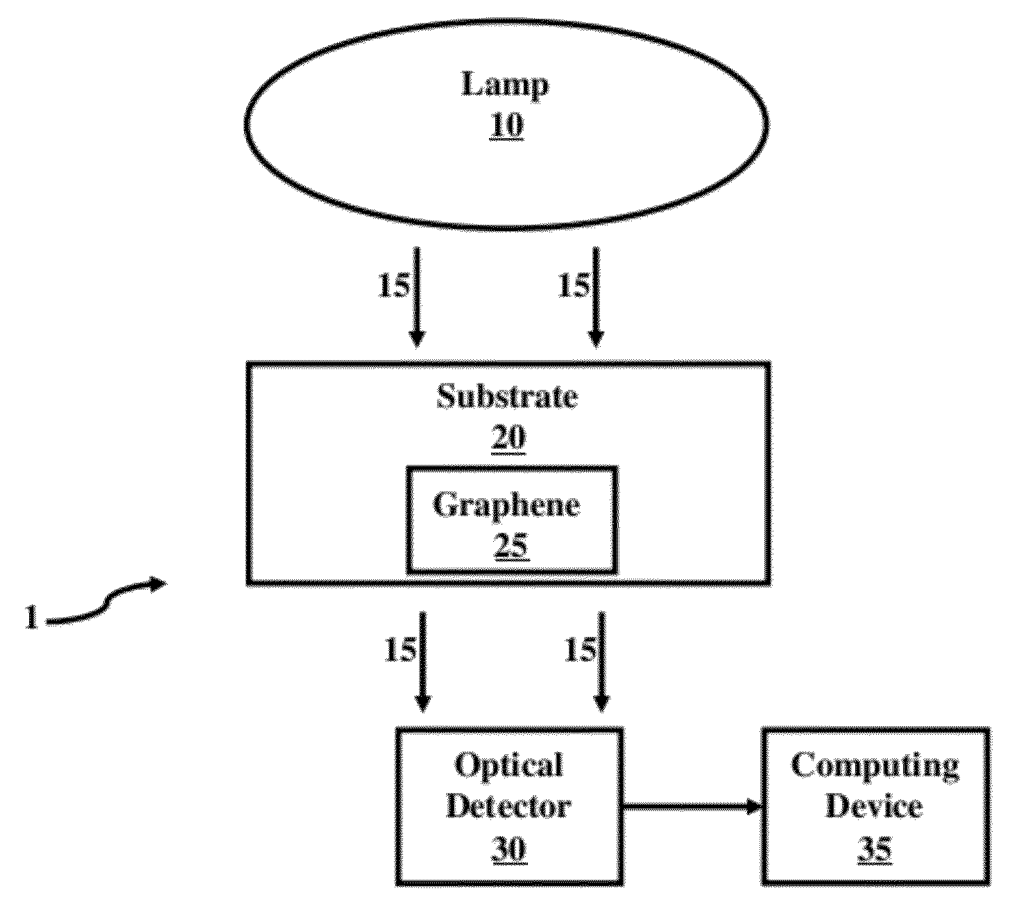
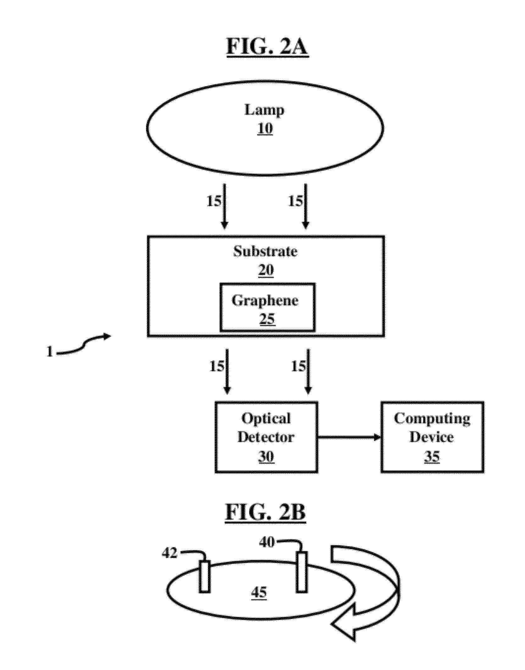
[0018]Referring now to the drawings, and more particularly to FIGS. 1 through 7, where similar reference characters denote corresponding features consistently throughout the figures, there are shown embodiments herein. The production of high-quality graphene and the manufacture of semiconductor...


PUM


Abstract

A method and system includes a first substrate and a second substrate, each substrate comprising a predetermined baseline transmittance value at a predetermine wavelength of light, processing regions on the first substrate by combinatorially varying at least one of materials, process conditions, unit processes, and process sequences associated with the graphene production, performing a first characterization test on the processed regions on the first substrate to generate first results, processing regions on a second substrate in a combinatorial manner by varying at least one of materials, process conditions, unit processes, and process sequences associated with the graphene production based on the first results of the first characterization test, performing a second characterization test on the processed regions on the second substrate to generate second results, and determining whether at least one of the first substrate and the second substrate meet a predetermined quality threshold based on the second results.

Description

BACKGROUND[0001]1. Technical Field[0002]The embodiments herein generally relate to semiconductor processing and characterization, and more specifically, to an improved system and method for uniformity testing of semiconductor substrates.[0003]2. Description of the Related Art[0004]The ability to process uniformly across a monolithic substrate and / or across a series of monolithic substrates is advantageous for manufacturing efficiency and cost effectiveness, as well as repeatability and control. However, uniform processing across an entire substrate can be disadvantageous when optimizing, qualifying or investigating new materials, new processes, and / or new process sequence integration schemes, since the entire substrate is nominally made the same using the same materials, processes, and process sequence integration schemes. Each processed substrate generally represents, in essence, only one possible variation per substrate. Thus, the full wafer uniform processing under conventional p...

Claims


Application Information

Patent Timeline
IPC IPC(8): G06F19/00H01L21/66
CPCG01N21/59H01L21/02491H01L21/02527H01L29/1606H01L22/12H01L22/20H01L21/0262
Inventor CHEN, CHARLENECHIANG, TONY P.LANG, CHI-IWANG, YUN
Owner INTERMOLECULAR
Why Eureka
Try Eureka