Infrared sensor

Inactive Publication Date: 2007-10-16
HAMAMATSU PHOTONICS KK
View PDF20 Cites 39 Cited by
  • Summary
  • Abstract
  • Description
  • Claims
  • Application Information

AI Technical Summary

Benefits of technology

[0011]Since a thermocouple is formed by stacking a polysilicon layer and an aluminum layer, the thermocouple is small, and a plurality of thermocouples can be places in series can be increased. Since the multilayered structure of the polysilicon layer and aluminum layer ranges from above a concavity to above a substrate, the mechanical strength of the thin concavity can be increased. Since the infrared absorption layer is formed to cover first junctions formed in the thermocouples, heat generated in the infrared absorption layer can be efficiently transmitted to the thermocouples.
[0012]The infrared sensor of the present invention may be characterized in that the substrate is made of silicon, and the concavity is formed by etching. Since the concavity is formed by etching, the shape of the concavity can be accurately implemented.
[0013]The infrared sensor of the present invention may be cha

Problems solved by technology

In addition, since a infrared absorbing film 105 and the thermocouples are formed apart from each other, heat generated in the infrared absorbing film 105 is no

Method used


Image

  • Infrared sensor
  • Infrared sensor
  • Infrared sensor

Examples


Example

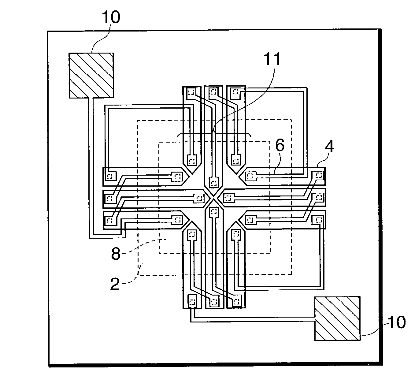
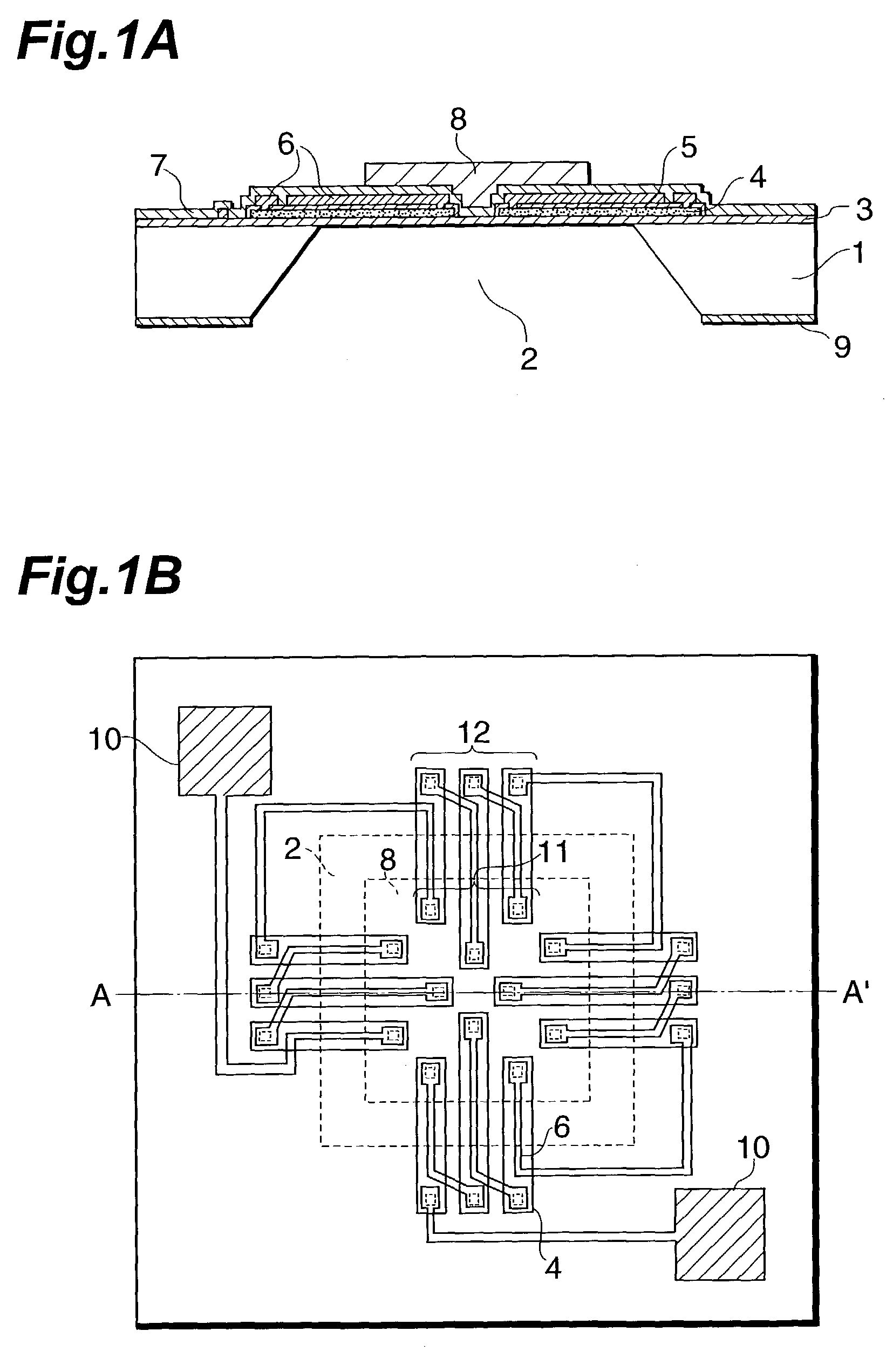
[0024]A section and thermopile patterns of an infrared sensor according to the first embodiment are shown in FIGS. 1A and 1B. FIG. 1A is a sectional view taken along A-A′ in FIG. 1B. As shown in FIG. 1A, the support member of a diaphragm structure has a silicon substrate 1 having a concavity 2, and a support film 3 which is supported by the silicon substrate 1. A polysilicon film 4 in which an n- or p-type impurity is doped at 1018 to 1020 cm−3 and an aluminum film 6 via an SiO2 film 5 serving as an insulating film are stacked on the support film 3. The polysilicon film 4 and aluminum film 6 are connected by an opening portion of the SiO2 film 5 to form a junction. The exposed surfaces of the support film 3 and thermocouples are coated with a passivation film 7 made of SiN. A infrared absorbing film 8 is formed on the passivation film 7 above the concavity 2.

[0025]Note that the passivation film 7 may be an insulating film such as an SiO2 or polyimide film. A blackened resin is used ...

Example

[0032]The thermopile patterns of an infrared sensor according to the second embodiment are shown in FIG. 2. The infrared sensor of the second embodiment is obtained by widening the polysilicon film 4 of the infrared sensor of the first embodiment shown in FIG. 1B and tapering the distal end of the polysilicon film 4 above the concavity 2.

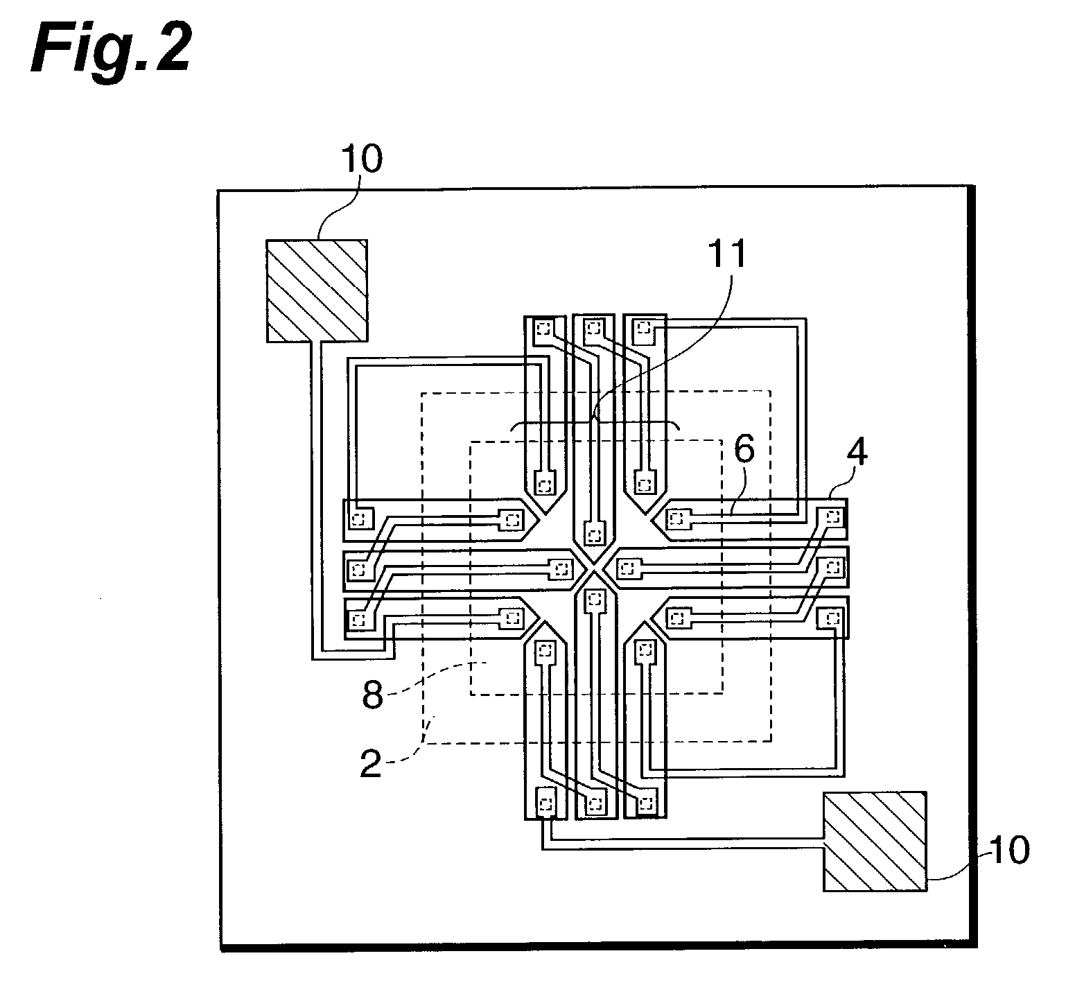
[0033]When a semiconductor material such as polysilicon is used as a thermoelectronic material, the resistance of the thermopile increases because of the high resistivity, and accordingly, noise increases. According to the infrared sensor of the second embodiment, since a polysilicon film 4 and an aluminum film 6 are stacked, the width of the polysilicon film 4 can be increased in each of thermocouples in number equal to or more than the prior art shown in FIG. 7. Hence, the resistance of the thermocouple can be reduced, and the S / N ratio can be increased by suppressing thermal noise. Alternatively, a design is also possible in which the number of t...

Example

[0035]A section and thermopile patterns of an infrared sensor according to the third embodiment are shown in FIGS. 3A and 3B. The infrared sensor of the third embodiment is obtained by changing the shape of the concavity 2 of the infrared sensor according to the first embodiment shown in FIG. 1A. More specifically, as shown in FIG. 3A that shows a section taken along B-B′ in FIG. 3B, in the third embodiment, the lower side of a concavity 2 is closed by a silicon substrate 1, etching holes 13 are formed at four portions of a passivation film 7 on an upper surface, and the concavity 2 is formed under the support film 3, unlike the first embodiment in which the lower side of the concavity 2 is open.

[0036]A method of forming the concavity 2 in the infrared sensor of the third embodiment will be described. First, a polysilicon sacrificial layer (not shown) having the same size as that of the concavity 2 is formed on the support film 3 side of a silicon substrate 1. After a support film 3...


PUM


Abstract

An infrared sensor of this invention is characterized by including a support member including a support film and a substrate that supports the support film, a polysilicon film which ranges from above a concavity to above the substrate, SiO2 which is formed on the polysilicon film and has a first junction hole above the concavity and a second junction hole above the substrate, an aluminum film which is connected to the polysilicon film through the first junction hole and connected to an adjacent polysilicon film through the second junction hole, and a heat absorption layer formed above the concavity to cover a portion above the first junction hole, wherein the aluminum film is stacked on the corresponding polysilicon film via the SiO2 above the concavity.

Description

RELATED APPLICATION[0001]This is a continuation-in-part application of application Ser. No. PCT / JP01 / 03077 filed on Apr. 10, 2001.BACKGROUND OF THE INVENTION[0002]1. Field of the Invention[0003]The present invention relates to an infrared sensor and, more particularly, to a thermopile infrared sensor.[0004]2. Related Background Art[0005]Conventional thermopile infrared sensors are shown in FIGS. 7 and 8. FIG. 7 shows the thermopile patterns of an infrared sensor. In this example, polysilicon 4 and aluminum 6, which are adjacent to each other, form a thermocouple. An infrared sensor shown in FIG. 8 is disclosed in Japanese Patent No. 2663612. In this example, a thermocouple made of a p-type semiconductor 106 and an n-type semiconductor 111 is formed on a cantilever 103. These infrared sensors measure the intensity of infrared rays incident on them on the basis of an electromotive force generated by the temperature difference between a hot junction and a cold junction of a thermocoupl...

Claims


Application Information

Patent Timeline
IPC IPC(8): G01J5/00H01L35/32G01J1/02G01J5/10G01J5/12
CPCG01J5/12G01J5/10H01L31/101
Inventor SHIBAYAMA, KATSUMI
Owner HAMAMATSU PHOTONICS KK
Why Eureka
Try Eureka