Data output driver and semiconductor memory device having the same

a data output and semiconductor technology, applied in the direction of logic circuit coupling/interface arrangement, pulse technique, instruments, etc., can solve the problems of cumbersome adjustment, cumbersome slope adjustment, and the inability to produce desired output data, so as to increase the delay time, decrease the delay time, increase the delay time

Inactive Publication Date: 2007-10-16
SAMSUNG ELECTRONICS CO LTD
View PDF14 Cites 16 Cited by
  • Summary
  • Abstract
  • Description
  • Claims
  • Application Information

AI Technical Summary

Benefits of technology

[0026]The rising transition slope adjuster may increase delay times of the first delay units in response to the first control signal when the driving capability of the pull-up driver increases in response to the third control signal, and decrease the delay times of the first delay units in response to the first control signal when the driving capability of the pull-up driver decreases in response to the third control signal. The falling transition slope adjuster increases delay times of the second delay units in response to the second control signal when the driving capability of the pull-down driver increases in response to the fourth control signal, and decreases the delay times of the second delay units in response to the second control signal when the driving capability of the pull-down driver decreases in response to the fourth control signal.
[0030]The rising transition slope adjuster may increase a delay time of each of the pull-up circuits in response to the first control signal when the driving capability of the pull-up driver increases in response to the third control signal, and decrease the delay time of each of the pull-up circuits in response to the first control signal when the driving capability of the pull-up driver decreases in response to the third control signal. The falling transition slope adjuster may increase a delay time of each of the pull-down circuits in response to the second control signal when the driving capability of the pull-down driver increases in response to the fourth control signal, and decrease the delay time of each of the pull-down circuits in response to the second control signal when the driving capability of the pull-down driver decreases in response to the fourth control signal.

Problems solved by technology

Thus, it is cumbersome to adjust the slope to be within the desired range by varying the delay times of the delay units 30-1 to 30-n and 40-1 to 40-n using the control signals CON1 and CON2.
Consequently, it is cumbersome to adjust the slopes again when the rising and falling transition slopes of the output data change in response to a change in driving capability in the conventional data output driver.
In some cases, the slopes may not be adjusted at all so that the desired output data cannot be produced.

Method used


Image

  • Data output driver and semiconductor memory device having the same
  • Data output driver and semiconductor memory device having the same
  • Data output driver and semiconductor memory device having the same

Examples


first embodiment

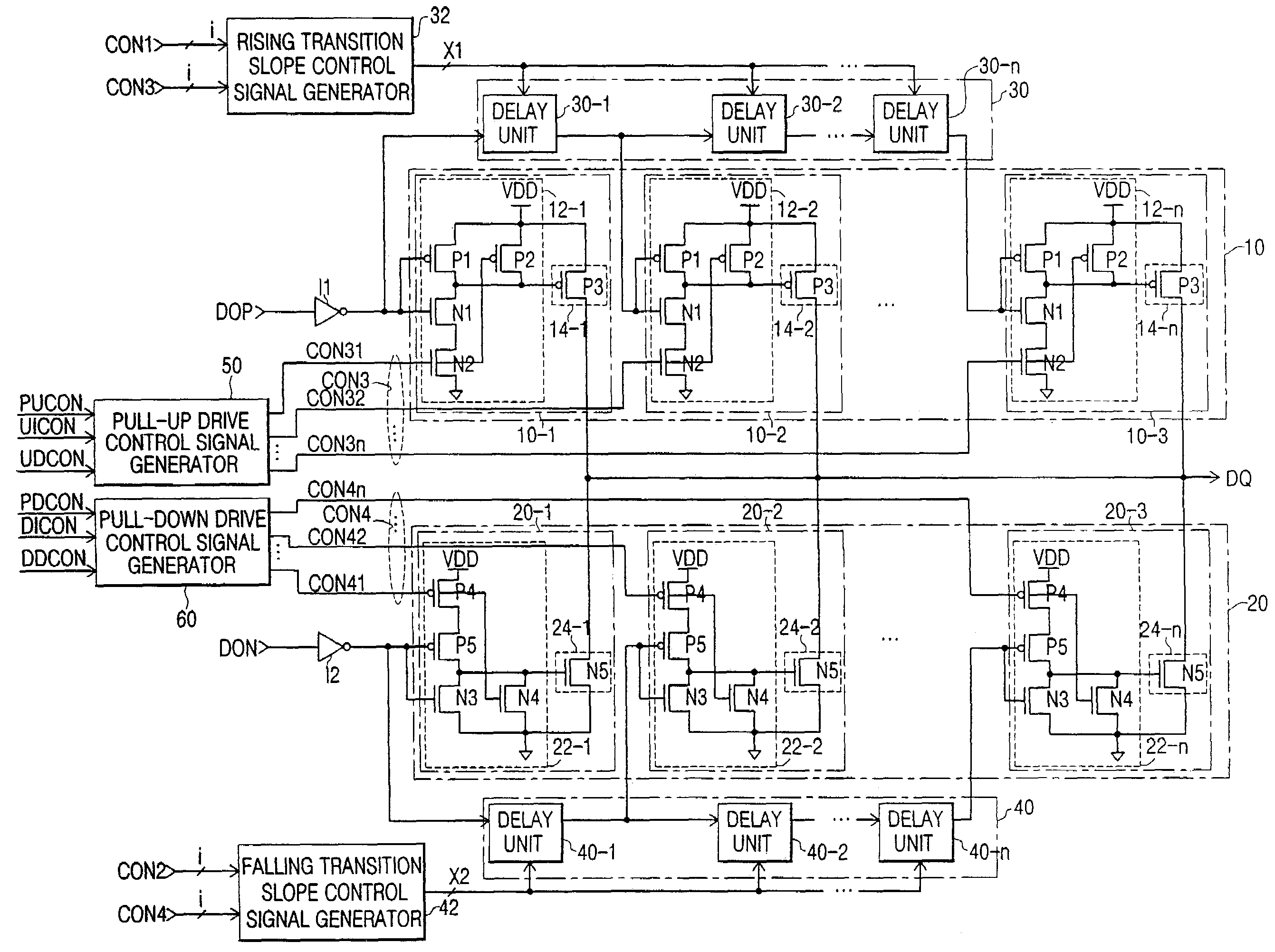
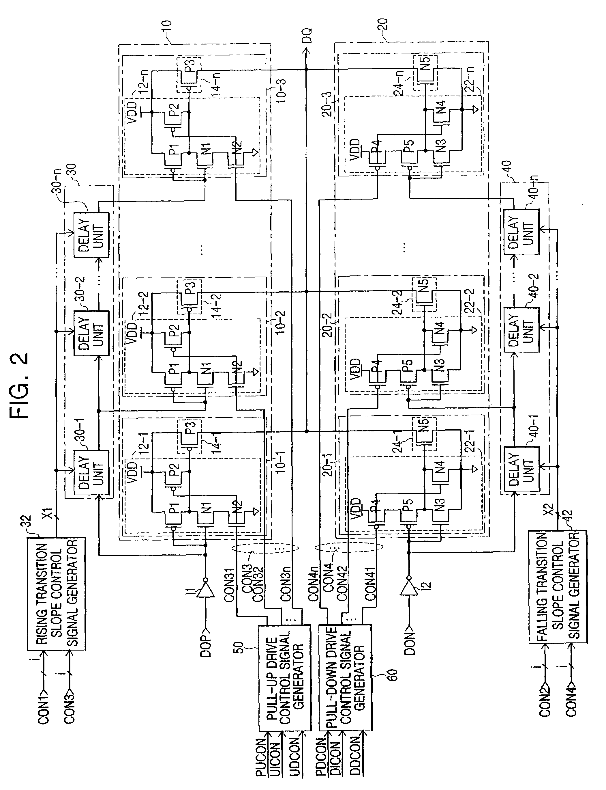
[0043]FIG. 2 is a diagram illustrating the structure of a data output driver in accordance with the present invention. In this embodiment, a rising transition slope control signal generator 32 and a falling transition slope control signal generator 42 are added to the data output driver shown in FIG. 1.

[0044]Functions of the same components as those shown in FIG. 1 will not be described, and only functions of additional components will be described hereinafter.

[0045]The rising transition slope control signal generator 32 varies delay times of delay units 30-1 to 30-n in response to control signals CON1 and CON3, and the falling transition slope control signal generator 42 varies delay times of delay units 40-1 to 40-n in response to control signals CON2 and CON4. The rising transition slope control signal generator 32 has an initial value set in response to the control signal CON1, and generates a control signal X1 that is increased or decreased with respect to the initial value in ...

second embodiment

[0052]FIG. 4 is a diagram illustrating the structure of a data output driver in accordance with the present invention, which replaces the delay units 30-1 to 30-n of FIG. 1 with delay units 30-1′ to 30-n′, and additionally includes resistors R11 to R1i connected in series between a power supply voltage and sources of PMOS transistors P2 of pull-up circuits 10-1 to 10-n, PMOS transistors P71 to P7i connected parallel to the respective resistors R11 to R1i, resistors R21 to R2i connected in series between a ground voltage and sources of NMOS transistors N4 of the pull-up circuits 10-1 to 10-n, and NMOS transistors N71 to N7n connected parallel to the respective resistors R21 to R2i. In addition, resistors R31 to R3i connected in series between the power supply voltage and sources of PMOS transistors P4 of pull-down circuits 20-1 to 20-n, and NMOS transistors N81 to N8i connected parallel to the respective resistors R31 to R3i are added to the circuit of FIG. 1.

[0053]Referring to FIG. ...

third embodiment

[0062]FIG. 5 is a diagram illustrating the structure of a data output driver in accordance with the present invention, which replaces the rising transition slope control signal generator 32 of FIG. 2 with a rising transition slope control signal generator 32′, and replaces the falling transition slope control signal generator 42 of FIG. 2 with a falling transition slope control signal generator 42′.

[0063]Functions of the same components as those shown in FIG. 2 will not be described, and only functions of added or replaced components will be described hereinafter.

[0064]The rising transition slope control signal generator 32′ has an initial value set in response to a control signal CON1, and generates a control signal X1 that has an increased value relative to the initial value in response to a pull-up rising control signal UICON and that has a decreased value relative to the initial value in response to a pull-up falling control signal UDCON. The falling transition slope control sig...


PUM


Abstract

A data output driver and a semiconductor memory device having the same are disclosed. This data output driver includes: a rising transition slope adjuster including a plurality of first delay units cascade-connected to each other and receiving data and generating delayed data, each of the first delay units having a delay time which varies in response to a first control signal; a falling transition slope adjuster including a plurality of second delay units cascade-connected to each other and receiving inverted data and generating delayed inverted data, each of the second delay units having a delay time which varies in response to a second control signal; a pull-up driver including a plurality of pull-up circuits, the driving capabilities of the pull-up circuits being adjustable in response to a third control signal, each pull-up circuit pulling-up output data in response to each of the data and the delayed data; and a pull-down driver including a plurality of pull-down circuits, the driving capabilities of the pull-down circuits being adjustable in response to a fourth control signal, each pull-down circuit pulling-down output data in response to each of the inverted data and the delayed inverted data, wherein the first control signal varies in response to the third control signal, and wherein the second control signal varies in response to the fourth control signal. Accordingly, the rising and falling transition slopes of the output data can be constant even when the driving capability is varied, so that output data having desired characteristics can be produced.

Description

CROSS-REFERENCE TO RELATED APPLICATION[0001]This application claims the benefit of Korean Patent Application No. 10-2005-0001876, filed Jan. 7, 2005, the disclosure of which is hereby incorporated herein by reference in its entirety.BACKGROUND OF THE INVENTION[0002]1. Field of the Invention[0003]The present invention relates to a data output driver, and more particularly, to a data output driver and a semiconductor memory device having the same which can adjust driving capability.[0004]2. Description of the Related Art[0005]A conventional data output driver includes a pull-up driver composed of a predetermined number of pull-up circuits and a pull-down driver composed of a predetermined number of pull-down circuits, and generates output data. Driving capability can be controlled by adjusting the number of enabled pull-up circuits and the number of enabled pull-down circuits constituting the pull-up driver and the pull-down driver, respectively, and the slopes of rising and falling t...

Claims


Application Information

Patent Timeline
Patent Type & Authority Patents(United States)
IPC IPC(8): H03B1/00H03K3/00
CPCG11C7/1051H03K19/0005H03K17/164G11C7/1057G11C7/10
Inventor LEE, DONG-JIN
Owner SAMSUNG ELECTRONICS CO LTD
Why Eureka
Try Eureka