Pixel clock generation device causing state transition of pixel clock according to detected state transition and phase data indicating phase shift amount

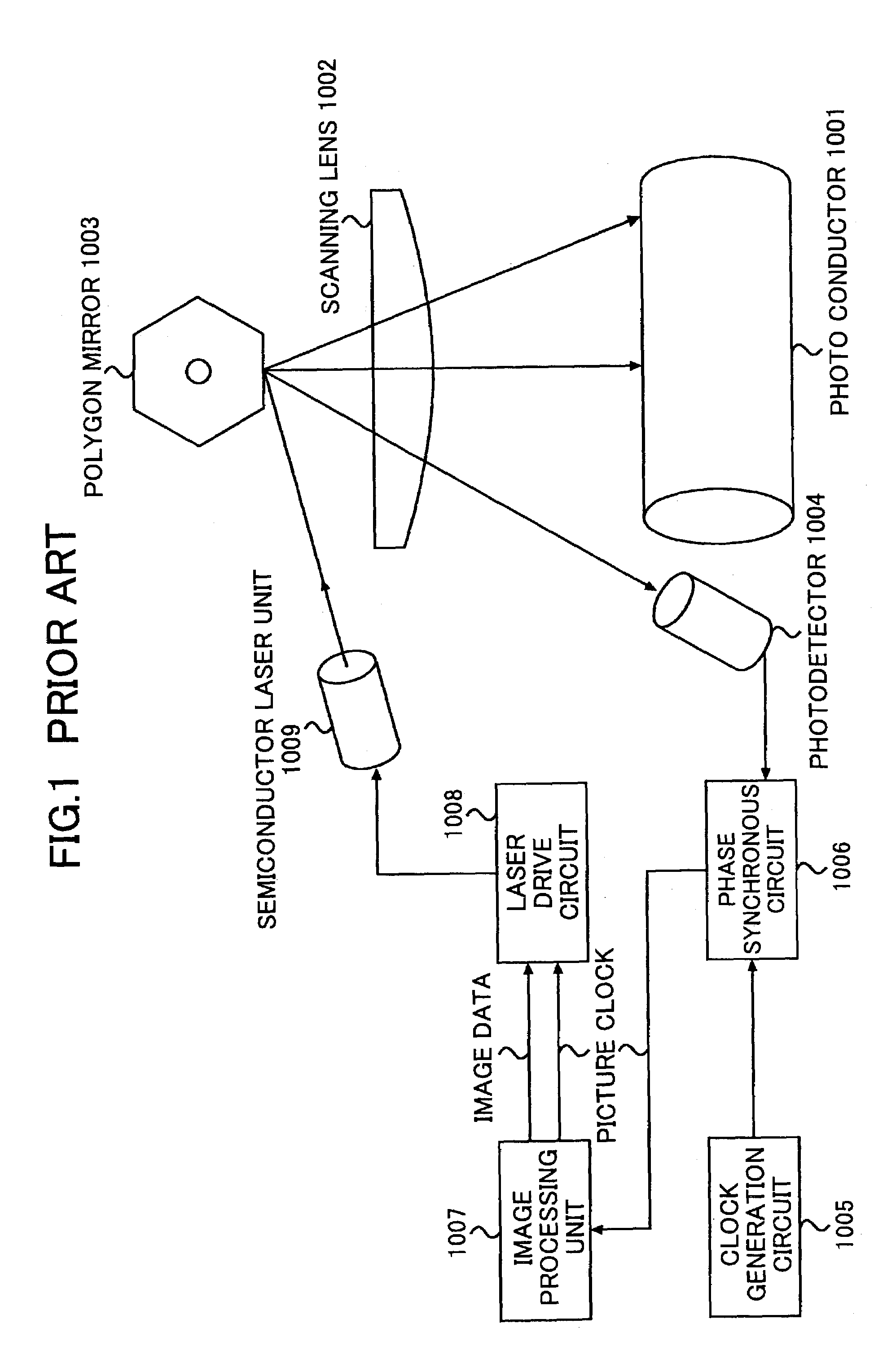
a generation device and state transition technology, applied in the direction of visual presentation, instruments, printing, etc., can solve the problems of irregular scanning speed of optical spots (i.e., scanning beams) on scanned surfaces, deterioration of image quality, and difference in scanning width of optical spots corresponding to respective light-emitting sources on scanned mediums

Inactive Publication Date: 2007-10-16
RICOH KK
View PDF19 Cites 82 Cited by
  • Summary
  • Abstract
  • Description
  • Claims
  • Application Information

AI Technical Summary

Benefits of technology

[0011]It is a general object of the present invention to provide an improved and useful pixel clock generation device, a laser scanning device, and an image forming device in which the above-mentioned problems are eliminated.
[0012]A more specific object of the present invention is to provide a pixel clock generation device having a simple structure which enables a highly precise and detailed phase control of a pixel clock, and to provide a laser scanning device and an image forming device including the pixel clock generation device.
[0014]According to the present invention, a highly precise phase control of the pixel clock can be performed with a simple structure.
[0016]According to the present invention, the detection signal can be generated easily according to the high-frequency clock.
[0018]According to the present invention, a more detailed phase control of the pixel clock can be performed with a simple structure.

Problems solved by technology

However, the configuration using the rotating deflector has a problem that a distance between a deflective reflection plane and a rotation axis in this deflector varies, and accordingly, a scanning speed of the optical spot (i.e., a scanning beam) scanning a scanned surface becomes irregular.
This scanning speed irregularity causes fluctuation in an image, resulting in a deteriorated image quality.
Further, when a multi-beam optical system is used as a light source, a difference in oscillation wavelengths of light-emitting sources of the multi-beam optical system causes exposure displacements, resulting in a difference in scanning widths of optical spots corresponding to the respective light-emitting sources on a scanned medium.
However, the above-mentioned conventional technique of changing the frequency of the picture clock (which is referred to as a frequency modulation method) involves a complicatedly structured picture clock control part.
Additionally, this complication increases as a frequency modulation width becomes small.
Thus, the frequency modulation method according to the conventional technique has a problem that a fine control cannot be performed.

Method used


Image

  • Pixel clock generation device causing state transition of pixel clock according to detected state transition and phase data indicating phase shift amount
  • Pixel clock generation device causing state transition of pixel clock according to detected state transition and phase data indicating phase shift amount
  • Pixel clock generation device causing state transition of pixel clock according to detected state transition and phase data indicating phase shift amount

Examples


embodiment 1

OPERATION OF EMBODIMENT 1

[0081]Next, a description will be given, with reference to a timing chart of FIG. 7, of operations of the pixel clock generation part 120. FIG. 7 shows examples of respective cases where phase shift amounts are ‘0’, ‘−1’ and ‘+1’. Besides, Table 2 below shows correspondences between the phase shift amounts and the phase data.

[0082]

TABLE 2Phase shift amountPhase data0 (no phase shift)011Advance 1 / 8 PCLK100Advance 2 / 8 PCLK101Advance 3 / 8 PCLK110Delay 1 / 8 PCLK010Delay 2 / 8 PCLK001Delay 3 / 8 PCLK000

[0083]Phase Shift Amount=0

[0084]First, a description will be given of the case of generating the pixel clock (PCLK) with the phase shift amount being ‘0’. In this case, the phase data “3” is supplied to the control signal generation circuit 123 at a timing t1 synchronous with a rise of the pixel clock (PCLK). At the same timing t1, the rise of the pixel clock (PCLK) is detected by the transition detection circuit 122 so that a detection signal is generated, and is suppli...

embodiment 2

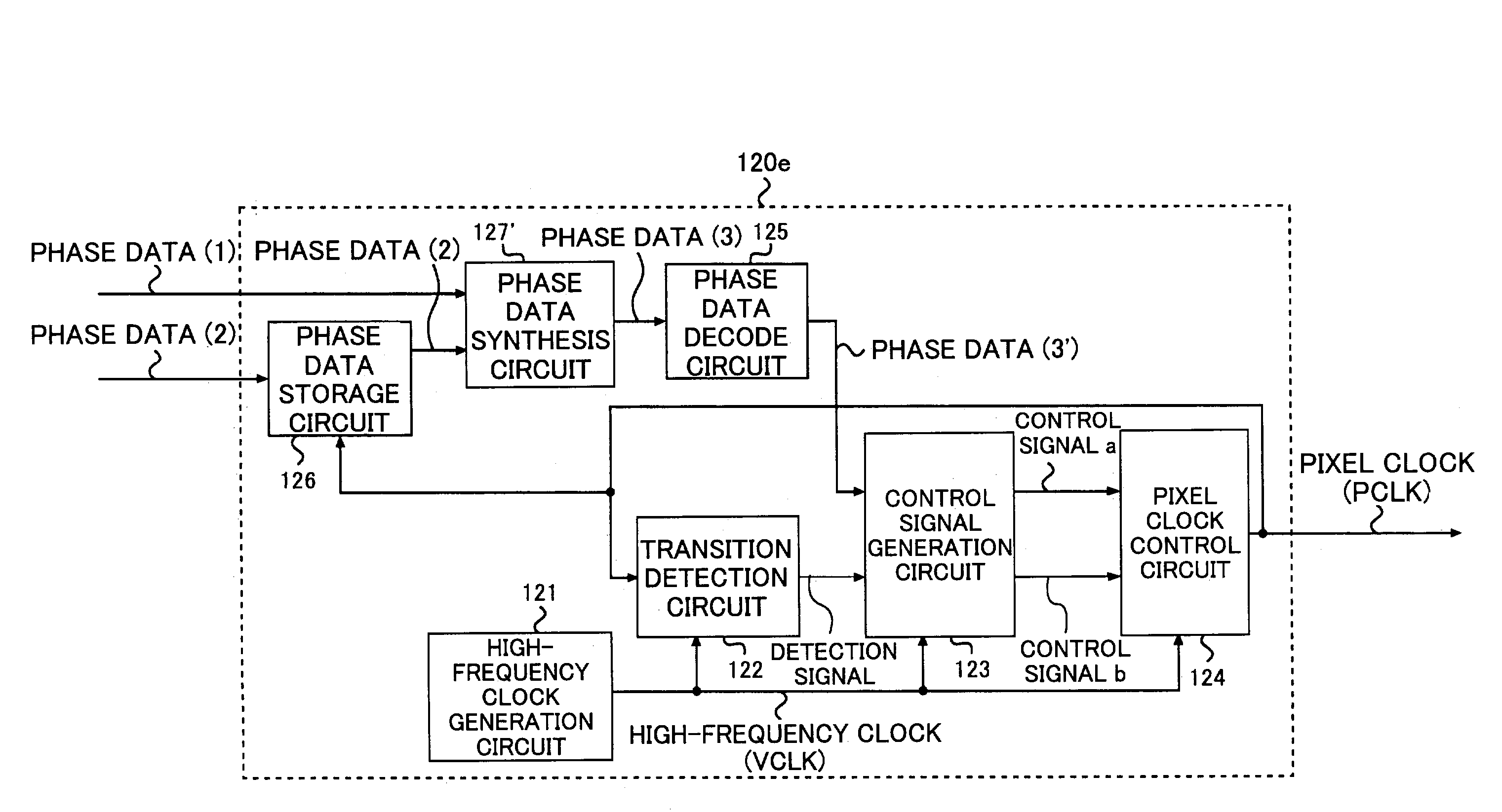
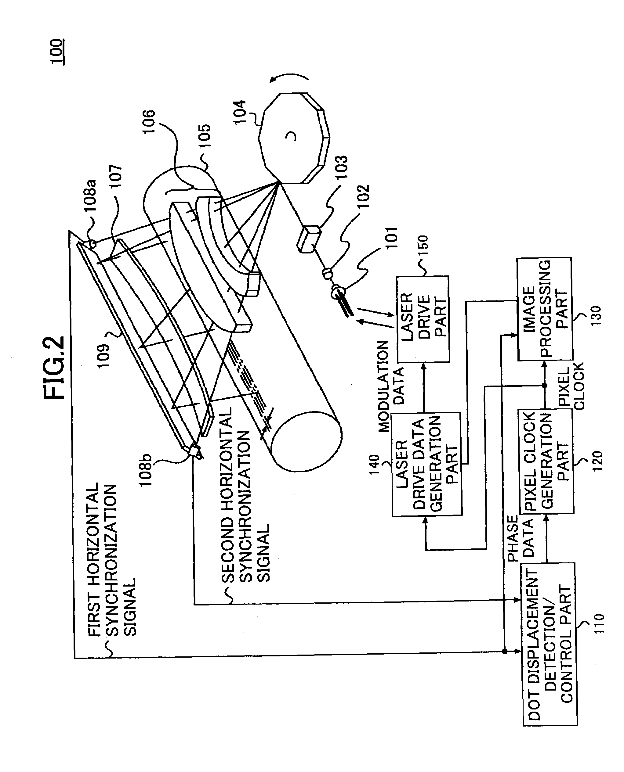
[0099]Next, a description will be given of another structure of the pixel clock generation part 120 according to the foregoing first embodiment as a second embodiment according to the present invention. FIG. 8 is a block diagram showing the structure of a pixel clock generation part 120a according to the present second embodiment.

[0100]As shown in FIG. 8, the pixel clock generation part 120a further comprises a phase data decode circuit 125 in addition to the structure of the pixel clock generation part 120 according to the foregoing first embodiment. This phase data decode circuit 125 converts phase data (1) from outside (for example, the dot displacement detection / control part 110 shown in FIG. 2) into phase data (1′) inside the pixel clock generation part 120a. In the present embodiment, it is assumed that the phase shift amounts and the phase data (1) outside have correspondences as shown in Table 3 below.

[0101]

TABLE 3Phase shift amountPhase data (1)0 (no phase shift)000Advance ...

embodiment 3

[0106]Next, a description will be given of another structure of the pixel clock generation part 120 according to the foregoing first embodiment as a third embodiment according to the present invention. FIG. 9 is a block diagram showing the structure of a pixel clock generation part 120b according to the present third embodiment.

[0107]As shown in FIG. 9, the pixel clock generation part 120b further comprises a phase data storage circuit 126 for storing a plurality of phase data, in addition to the structure of the pixel clock generation part 120 according to the foregoing first embodiment. A plurality of phase data are preset in this phase data storage circuit 126 from outside and so forth. Accordingly, upon operation, the phase data storage circuit 126 reads the phase data one by one in synchronization with the pixel clock (PCLK), and supplies the phase data to the control signal generation circuit 123. Besides, the phase data storage circuit 126 includes an address counter.

[0108]As...


PUM


Abstract

A transition detection circuit detects a transition of a state of a pixel clock, and outputs a detection signal according to a timing of the detected state transition. A control signal generation circuit generates a control signal according to the detection signal and phase data indicating a transition timing of the pixel clock. A pixel clock control circuit causes the state of the pixel clock to transit according to the control signal.

Description

BACKGROUND OF THE INVENTION[0001]1. Field of the Invention[0002]The present invention generally relates to a pixel clock generation device, a laser scanning device, and an image forming device, and more particularly, to a pixel clock generation device generating a pixel clock, a laser scanning device and an image forming device including the pixel clock generation device.[0003]2. Description of the Related Art[0004]FIG. 1 shows a general configuration of an image forming device, such as a laser printer and a digital composite device. In FIG. 1, a laser light emitted from a semiconductor laser unit 1009 undergoes a scanning by a rotating polygon mirror 1003, and is projected via a scanning lens 1002 on a photo conductor 1001 which is a scanned medium. The projected laser light forms an optical spot on the photo conductor 1001, thereby forming an electrostatic latent image on the photo conductor 1001. Additionally, the polygon mirror 1003 projects the laser light on a photodetector 10...

Claims


Application Information

Patent Timeline
Patent Type & Authority Patents(United States)
IPC IPC(8): B41J2/435B41J2/47G06K15/12H04N1/04
CPCB41J2/473H04N1/04G06K15/1219
Inventor NIHEI, YASUHIROISHIDA, MASAAKI
Owner RICOH KK
Why Eureka
Try Eureka