
Alignment system and lithographic apparatus equipped with such an alignment system

a technology of alignment system and lithographic apparatus, which is applied in the field of alignment system, can solve the problems of affecting the quality of alignment, and affecting the quality of alignment, and achieves the effect of improving the quality of alignmen

Inactive Publication Date: 2007-10-16
ASML NETHERLANDS BV
View PDF2 Cites 12 Cited by
  • Summary
  • Abstract
  • Description
  • Claims
  • Application Information

AI Technical Summary

Benefits of technology

The present invention provides an alignment system that can improve the quality of alignment when using deformed alignment markers with a specific wavelength range of radiation. This is achieved by designing a marker structure with alternating line elements and trench elements that have a variation in pitch value over the sequence length of the marker. The alignment system can illuminate the marker structure with an illumination beam and generate a diffraction pattern comprising diffracted beams, which can be used to determine the alignment of the substrate. The alignment system can also obtain alignment information from the diffraction pattern to improve the accuracy of the alignment.

Problems solved by technology

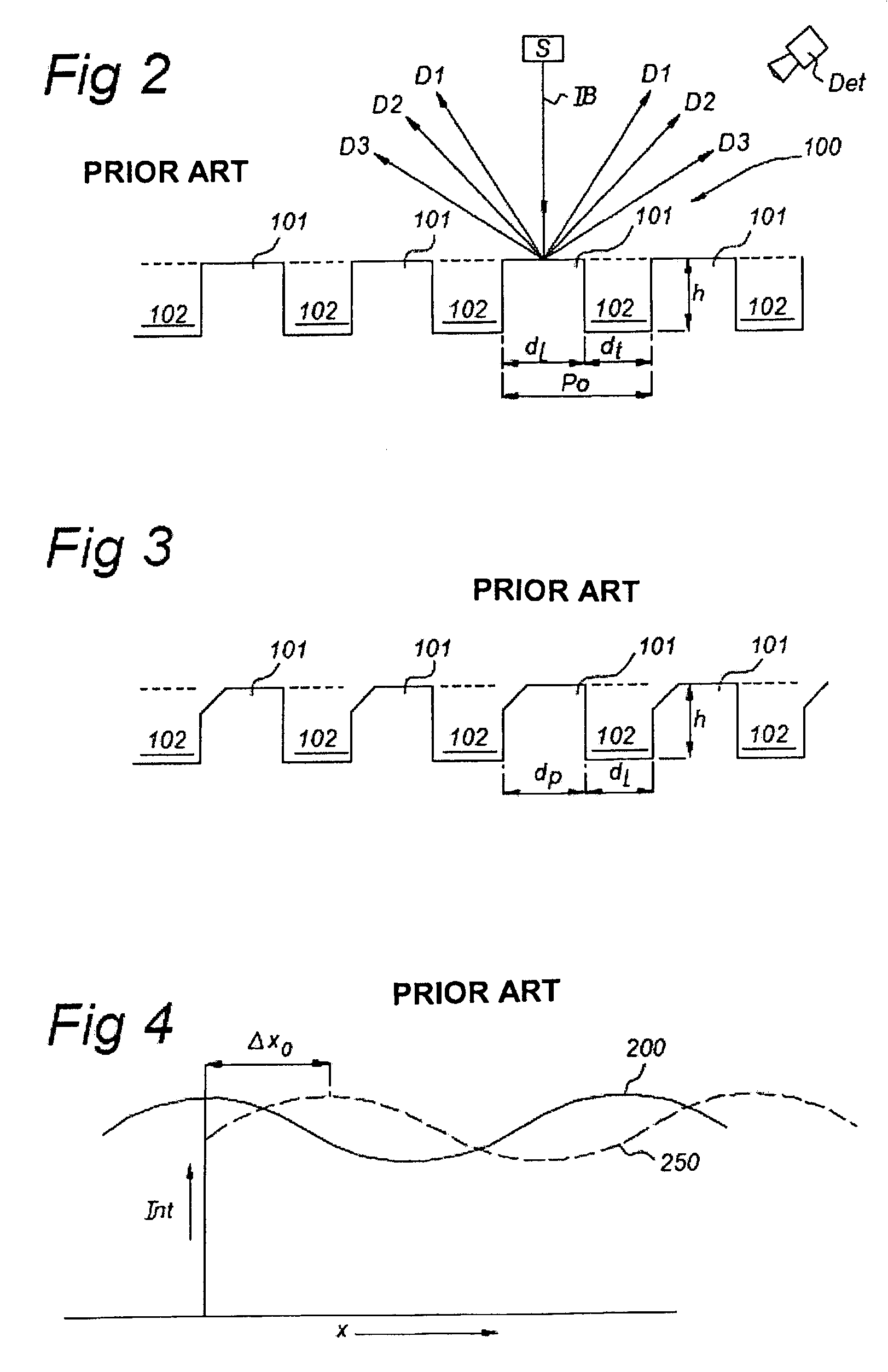
However, in practice the alignment procedure is hindered by a deformation of the alignment grating(s).
The asymmetry of the lines and / or trenches influence the orders in the diffraction pattern, which may lead to an erroneous shift of the aligned position as calculated from the diffraction pattern.
However, use of such a broad-band system may not be compatible for a lithographic apparatus in which the broad-band radiation must pass an optical path to reach the alignment marker.
Other wavelengths may not pass the optical path as desired leading to a flawed radiation beam for diffraction.
Moreover, a broad-band radiation may also cause undesired thermal effects in the optical path that affect the imaging quality of the lithographic apparatus.

Method used


Image

  • Alignment system and lithographic apparatus equipped with such an alignment system
  • Alignment system and lithographic apparatus equipped with such an alignment system
  • Alignment system and lithographic apparatus equipped with such an alignment system

Examples


embodiments

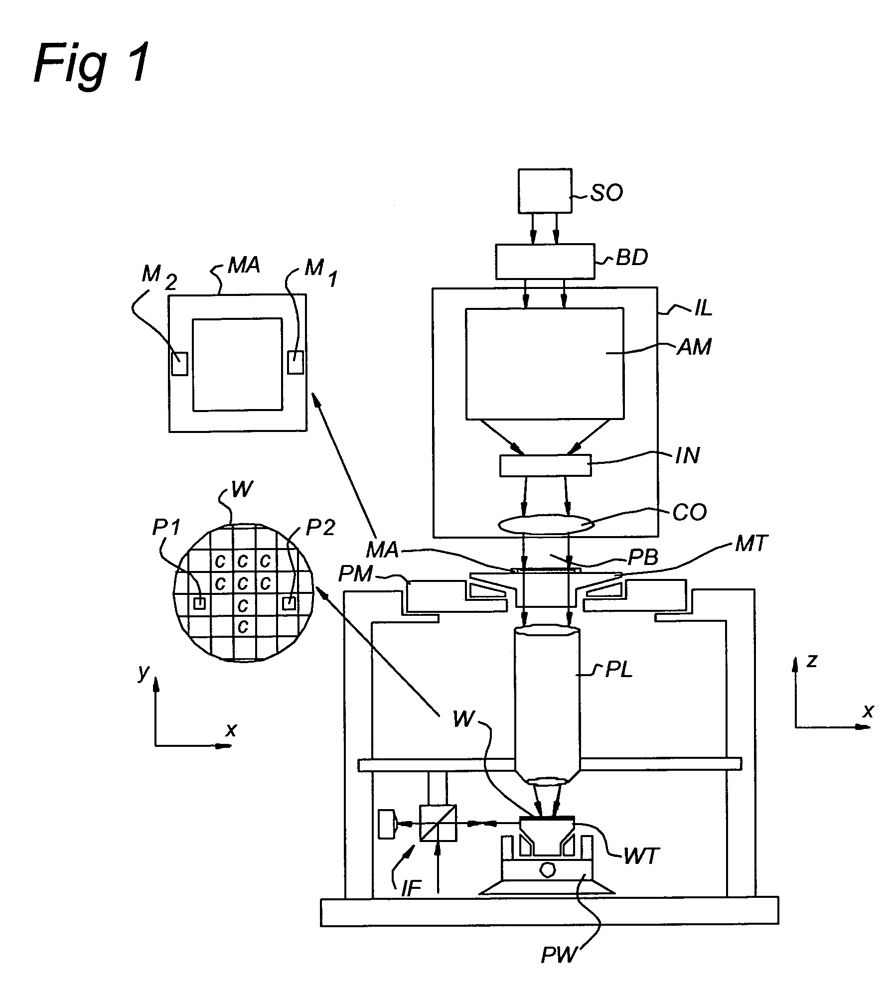
[0034]FIG. 1 schematically depicts a lithographic apparatus according to a particular embodiment of the invention. The apparatus comprises:.[0035]an illumination system (illuminator) IL for providing a projection beam PB of radiation (e.g. UV radiation).[0036]a first support structure (e.g. a mask table) MT for supporting patterning device (e.g. a mask) MA and connected to first positioner PM for accurately positioning the patterning device with respect to item PL;[0037]a substrate table (e.g. a wafer table) WT for holding a substrate (e.g. a resist-coated wafer) W and connected to second positioner PW for accurately positioning the substrate with respect to item PL; and[0038]a projection system (e.g. a refractive projection lens) PL for imaging a pattern imparted to the projection beam PB by patterning device MA onto a target portion C (e.g. comprising one or more dies) of the substrate W.

[0039]As here depicted, the apparatus is of a transmissive type (e.g. employing a transmissive...


PUM

PropertyMeasurementUnit
wavelengthaaaaaaaaaa

Abstract

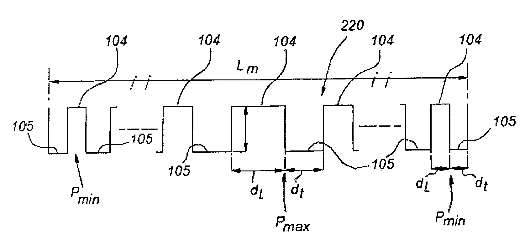
A marker structure on a substrate includes line elements and trench elements, the line elements and trench elements each having a length in a first direction and being arranged in an alternating repetitive sequence in a second direction perpendicular to the first direction, the alternating repetitive sequence having a sequence length, the marker structure having at least one pitch value, the at least one pitch value being the sum of a line width of one line element and a trench width of one trench element. A width of the line elements varies over the sequence length of the marker structure between a minimum line width value and a maximum line width value, while a width of the trench elements likewise varies over the sequence length of the marker structure between a minimum trench width value and a maximum trench width value. A duty cycle of a pair of a line element and an adjacent trench element is substantially constant over the sequence length of the marker structure. Thus, the pitch value varies from a minimum pitch value to a maximum pitch value over the sequence length.

Description

BACKGROUND OF THE INVENTION[0001]1. Field of the Invention[0002]The present invention relates generally to systems for aligning objects and certain embodiments relate more particularly to lithographic apparatus equipped with such an alignment system.[0003]2. Description of the Related Art[0004]A lithographic apparatus is a machine that applies a desired pattern onto a target portion of a substrate. Lithographic apparatus can be used, for example, in the manufacture of integrated circuits (ICs). In that circumstance, a patterning device, which is alternatively referred to as a mask or a reticle, may be used to generate a circuit pattern corresponding to an individual layer of the IC, and this pattern can be imaged onto a target portion (e.g. comprising part of, one or several dies) on a substrate (e.g. a silicon wafer) that has a layer of radiation-sensitive material (resist). In general, a single substrate will contain a network of adjacent target portions that are successively expo...

Claims


Application Information

Patent Timeline
Patent Type & Authority Patents(United States)
IPC IPC(8): G01B11/00G03B27/32G03B27/42G03C5/00G03F9/00H01L21/76H01L23/544
CPCG03F9/7076
Inventor PRESURA, CRISTIANVAN DER WERF, JAN EVERT
Owner ASML NETHERLANDS BV
Learn More