TDI detecting device, a feed-through equipment and electron beam apparatus using these devices

Active Publication Date: 2007-10-23
EBARA CORP
View PDF22 Cites 18 Cited by
  • Summary
  • Abstract
  • Description
  • Claims
  • Application Information

AI Technical Summary

Benefits of technology

[0010]The present invention has been made in the light of the problems associated with the prior art as discussed above, and an object thereof is to provide a TDI detecting device with which an effect from the distortion inherent to the optics of an image projecting

Problems solved by technology

In the prior art feed-through device 94 shown in FIGS. 13 and 14, if a number of pins used for the connection is not so much, even a small connecting force (resistance force) should be sufficient for mating the pins with the sockets, but if a large number of pins is used for the connection, a great connecting force should be necessary, which sometimes causes a problem that a semiconductor sensor to be connected by the feed-through device could be broken by this great connecting force.
In contrast, when a small number of pins is used for the connection, although there may occur no breakage in the semiconductor device owing to rather small connecting force, there has been another problem that, upon inspecting a wafer having an extended surface, the time r

Method used


Image

  • TDI detecting device, a feed-through equipment and electron beam apparatus using these devices
  • TDI detecting device, a feed-through equipment and electron beam apparatus using these devices
  • TDI detecting device, a feed-through equipment and electron beam apparatus using these devices

Examples


Example

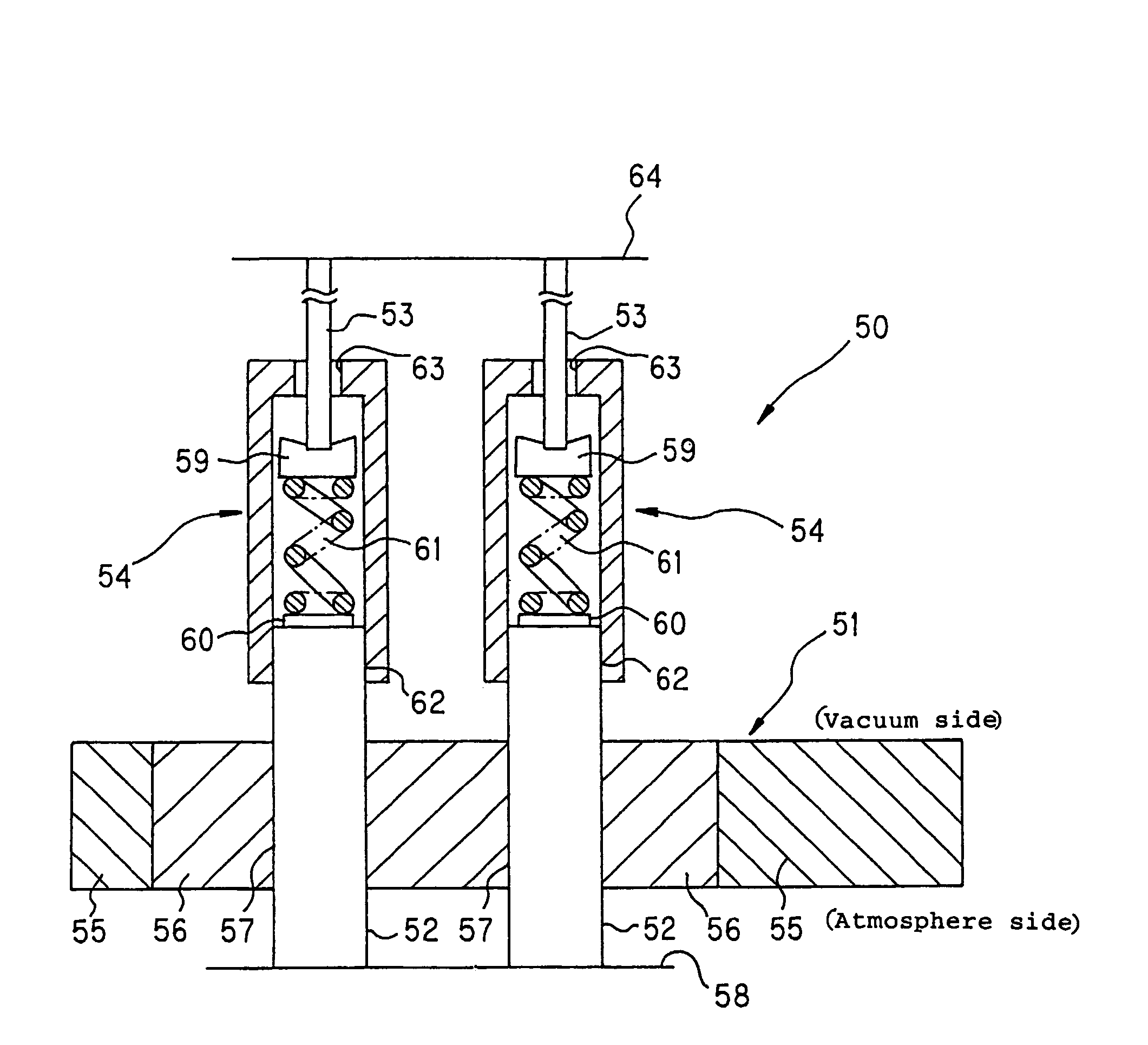
[0046]Preferred embodiments of the present invention will now be described with reference to the attached drawings.

(TDI Sensor)

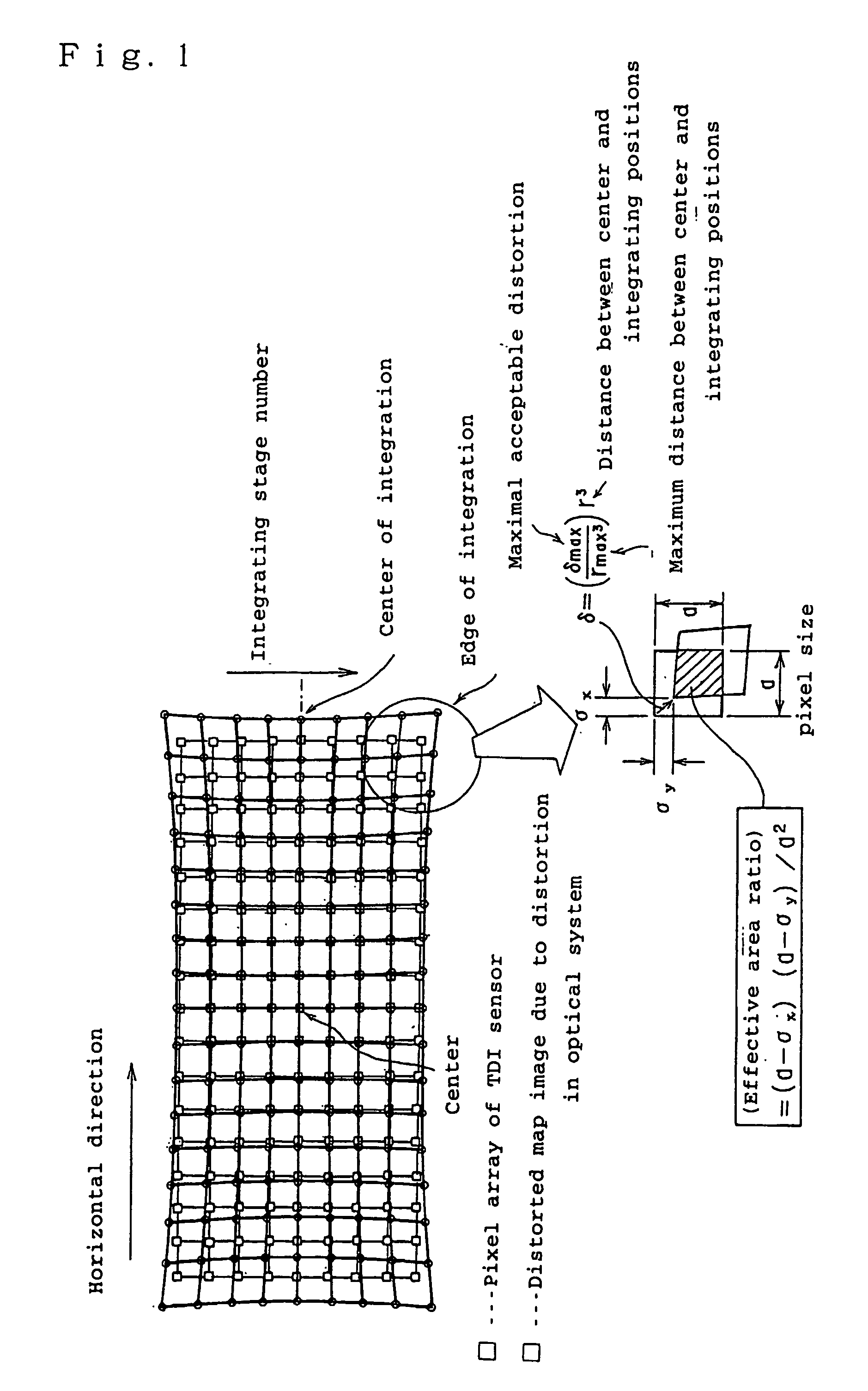
[0047]An embodiment for determining an optimized number of integration stages of a TDI sensor will be discussed below. Table 1 indicates a field of view, that is, a diagonal line length of a sensor effective region, and a maximal acceptable distortion across an entire field of view of a TDI sensor for different horizontal resolutions and different numbers of integration stages with a total number of the pixels thereof remained almost equal to that of an existing TDI sensor.

[0048]TABLE 1Maximal acceptableHorizontalNumber ofField of viewdistortionresolutionintegration stageμmδmax μm2048512337571.5410241024231482.227681366250523.225122048337574.76

[0049]It can be seen from the Table 1 that the field of view is minimized for the TDI sensor with the number of integration stages of 1024 and the maximal acceptable distortion becomes greater as the number of integrat...


PUM


Abstract

An electron beam apparatus comprises a TDI sensor (64) and a feed-through device (50). The feed-through device has a socket contact (54) for interconnecting a pin (52) attached to a flanged (51) for separating different environments. The other pin (53) making a pair with the pin (52) and the socket contact (54) together construct a connecting block, and the socket contact (54) has an elastic member (61). The pin (53) is connected with the TDI sensor (64), in which a pixel array has been adaptively configured based on the optical characteristic of an image projecting optical system. That sensor has a number of integration stages that can reduce the field of view of the image projecting optical system. Further, the number of integration stage may be determined such that the data rate of the TDI sensor would not be reduced but the number of pins would not be increased as much as possible. Preferably, the number of line count may be almost equal to the number of integration stages.

Description

TECHNICAL FIELD OF THE INVENTION[0001]The present invention relates to a TDI detecting device used to detect an electron image formed through a projection by an image projecting optical system, a feed-through device having a plurality of contact pins and functioning for realizing a high frequency response characteristic in such a condition having different gas pressures and / or different gas types, for example, a condition utilizing a vacuum environment and an atmospheric environment separately, and an electron beam apparatus utilizing the TDI detecting device equipped with said feed-through device, and also relates to a semiconductor device manufacturing method using said electron beam apparatus.BACKGROUND OF THE INVENTION[0002]FIG. 12 shows an electron beam apparatus of image projecting type according to a prior art, in which a primary electron beam is radiated onto a surface of a sample, and a secondary electron beam emitted from the surface of the sample is image-projected onto a...

Claims


Application Information

Patent Timeline
IPC IPC(8): H01R13/73G01N21/956G03F7/20H01J37/22H01J37/244H01L21/027H01R13/24H04N5/225
CPCG01N21/956H01J37/222H01J37/224H01J37/244H01R13/2421H04N5/2253Y10S439/935H01J2237/2447H01J2237/2445H04N23/54H01J37/22
Inventor HATAKEYAMA, MASAHIROSATAKE, TOHRUMURAKAMI, TAKESHIWATANABE, KENJINOJI, NOBUHARU
Owner EBARA CORP
Why Eureka
Try Eureka