Method for the production of a bipolar semiconductor component, especially a bipolar transistor, and corresponding bipolar semiconductor component

Inactive Publication Date: 2007-10-23
INFINEON TECH AG
View PDF9 Cites 6 Cited by
  • Summary
  • Abstract
  • Description
  • Claims
  • Application Information

AI Technical Summary

Benefits of technology

[0013]It is an object of the invention to specify an improved method for the production of a bipolar semiconductor component, especially a bi

Problems solved by technology

Since lithographic methods can only achieve resolutions of as far as 0.1 μm, this method is not suitable for scaled bipolar transistors in which the emitter is only a few 0.1 μm wide and the insulat

Method used


Image

  • Method for the production of a bipolar semiconductor component, especially a bipolar transistor, and corresponding bipolar semiconductor component
  • Method for the production of a bipolar semiconductor component, especially a bipolar transistor, and corresponding bipolar semiconductor component
  • Method for the production of a bipolar semiconductor component, especially a bipolar transistor, and corresponding bipolar semiconductor component

Examples


Example

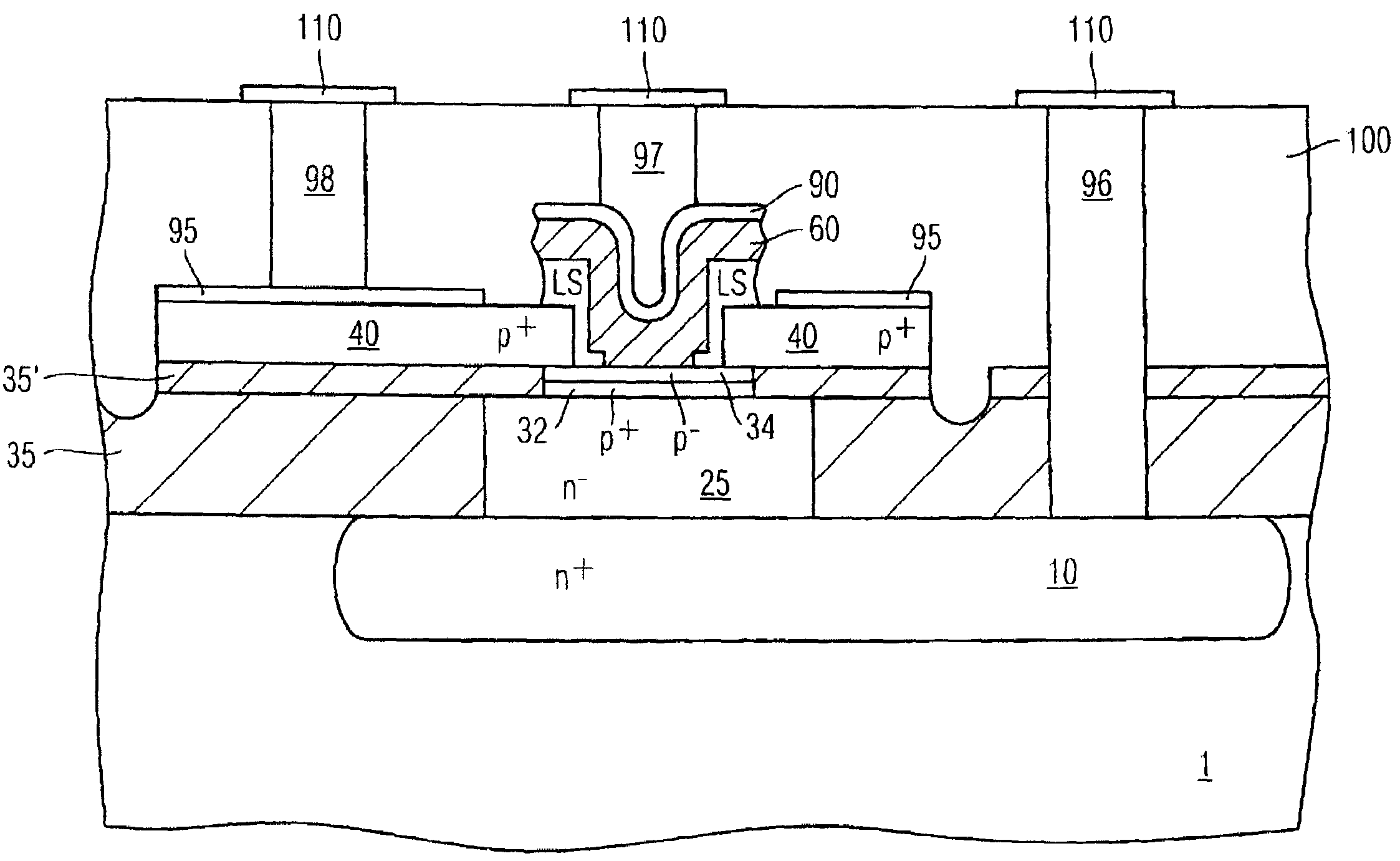
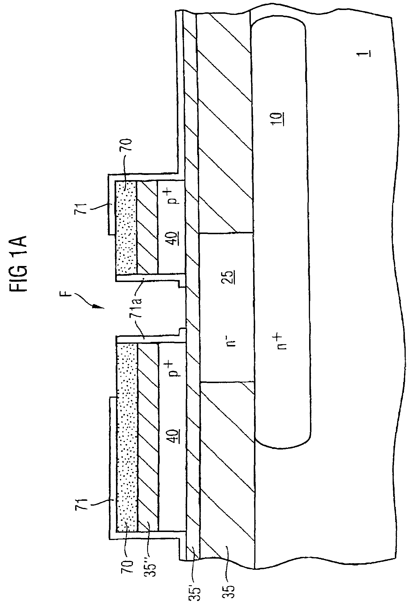
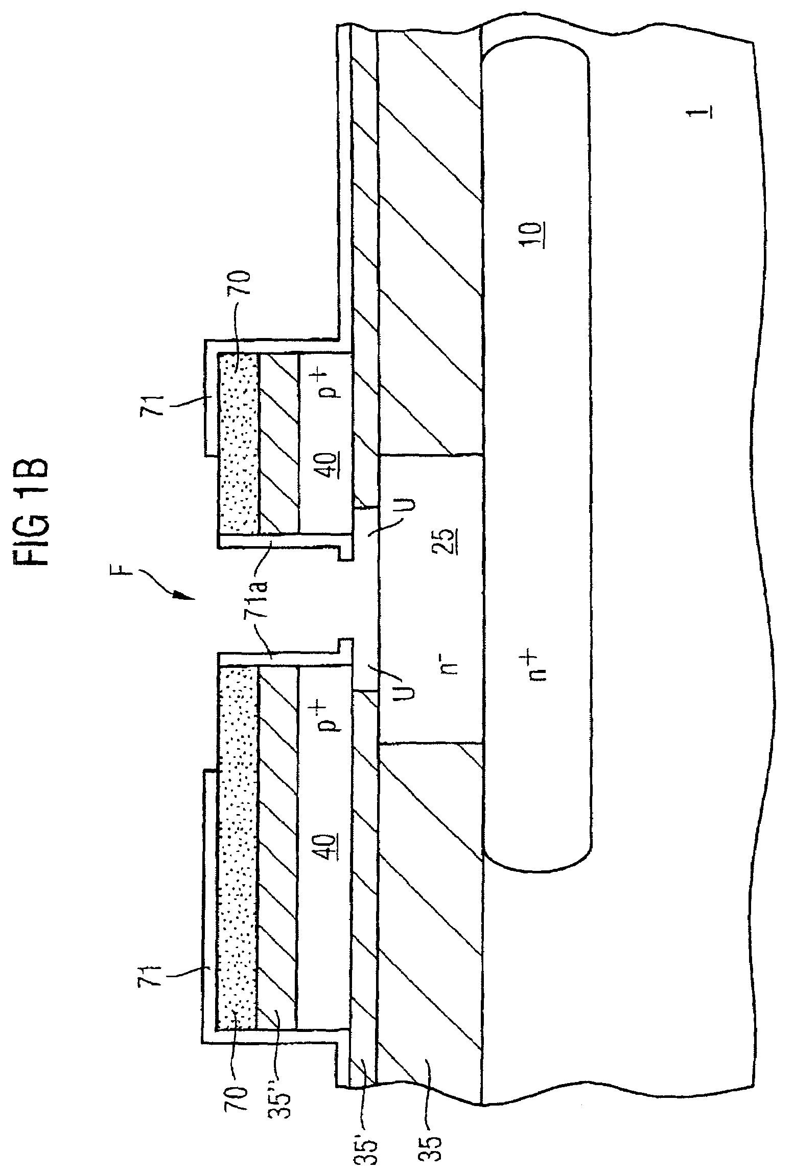
[0027]Identical reference symbols in the figures designate identical or identically acting elements.

[0028]The concepts on which the present invention is based commence at FIG. 3c. The emitter and base electrodes 60, 40 of the known DPSA transistor together with the intervening dielectric of the spacer 55′ form a capacitor, the capacitance Csp of which increases the emitter-base capacitance CBE of the transistor. The latter is one of the most important performance-determining variables of a bipolar transistor. Thus, the following holds true, e.g. for the transition frequency of a bipolar transistor:

[0029]12⁢π⁢⁢∫1=τ⁢∫+(RC+RE)⁢CBC+CBE+CBCIC⁢UT(Equation⁢⁢1)

where[0030]fT denotes transition frequency[0031]τf denotes transit time[0032]RC denotes collector resistance[0033]RE denotes emitter resistance[0034]CBC denotes base-collector capacitance[0035]CBE denotes base-emitter capacitance[0036]IC denotes collector current[0037]UT denotes thermal voltage.

[0038]It is evident that, for small coll...


PUM


Abstract

The invention relates to a method for producing a bipolar semiconductor element, especially a bipolar transistor, and a corresponding bipolar semiconductor component. The inventive method comprises the following steps: a first semiconductor area (32, 34) of a first conductivity type (p) is provided above a semiconductor substrate (1); a connecting area (40) of the first conductivity type (p<+>) is provided above the semiconductor area (32, 34); a first insulating area (35″) is provided above the connecting area (40); a window (F) is formed within the first insulating area (35″) and the connecting area (40) so as to at least partly expose the semiconductor area (32, 34); a sidewall spacer (80) is provided in the window (F) in order to insulate the connecting area (40); a second semiconductor area (60) of the second conductivity type (n+) is provided so as to cover the sidewall spacer (80) and a portion of the surrounding first insulating area (35″); the surrounding first insulating area (35″) and the sidewall spacer (80) are removed in order to form a gap (LS) between the connecting area (40) and the second semiconductor area (60); and the gap (LS) is sealed by means of a second insulating area (100) while a gaseous atmosphere or a vacuum atmosphere is provided inside the sealed gap (LS).

Description

RELATED APPLICATIONS[0001]This application is a continuation of PCT patent application number PCT / EP2004 / 003805, filed Apr. 8, 2004, which claims priority to German patent application number 10316529.0, filed Apr. 10, 2003, the disclosures of each of which are incorporated herein by reference in their entirety.TECHNICAL FIELD[0002]The present invention relates to a method for the production of a bipolar semiconductor component, especially a bipolar transistor, and a corresponding bipolar semiconductor component.BACKGROUND ART[0003]In order to electrically insulate the terminal regions of the emitter and base in bipolar transistors from one another, in principle two methods are available: firstly, the terminal regions may be defined with the aid of photolithography for the emitter and base regions and be patterned with the aid of etching technology. Such transistors are therefore called aligned transistors. The distance between emitter and base terminal is then given by the minimum a...

Claims


Application Information

Patent Timeline
IPC IPC(8): H01L21/331H01L29/06H01L29/732H01L29/737
CPCH01L29/0649H01L29/66242H01L29/7378H01L29/732H01L29/66287H01L29/7317
Inventor BOCK, JOSEFMEISTER, THOMASSTENGL, REINHARDSCHAFER, HERBERT
Owner INFINEON TECH AG
Why Eureka
Try Eureka