
Epitaxial wafer and method for manufacturing method

a manufacturing method and epitaxial wafer technology, applied in the field of epitaxial wafers, can solve the problems of difficult control of achieve the effect of improving the micro-roughness of the epitaxial wafer surfa

Inactive Publication Date: 2007-10-30
SUMITOMO MITSUBISHI SILICON CORP
View PDF5 Cites 8 Cited by
  • Summary
  • Abstract
  • Description
  • Claims
  • Application Information

AI Technical Summary

Benefits of technology

[0010]It is an object of the present invention to provide an epitaxial wafer with fewer pit defects in the epitaxial layer.
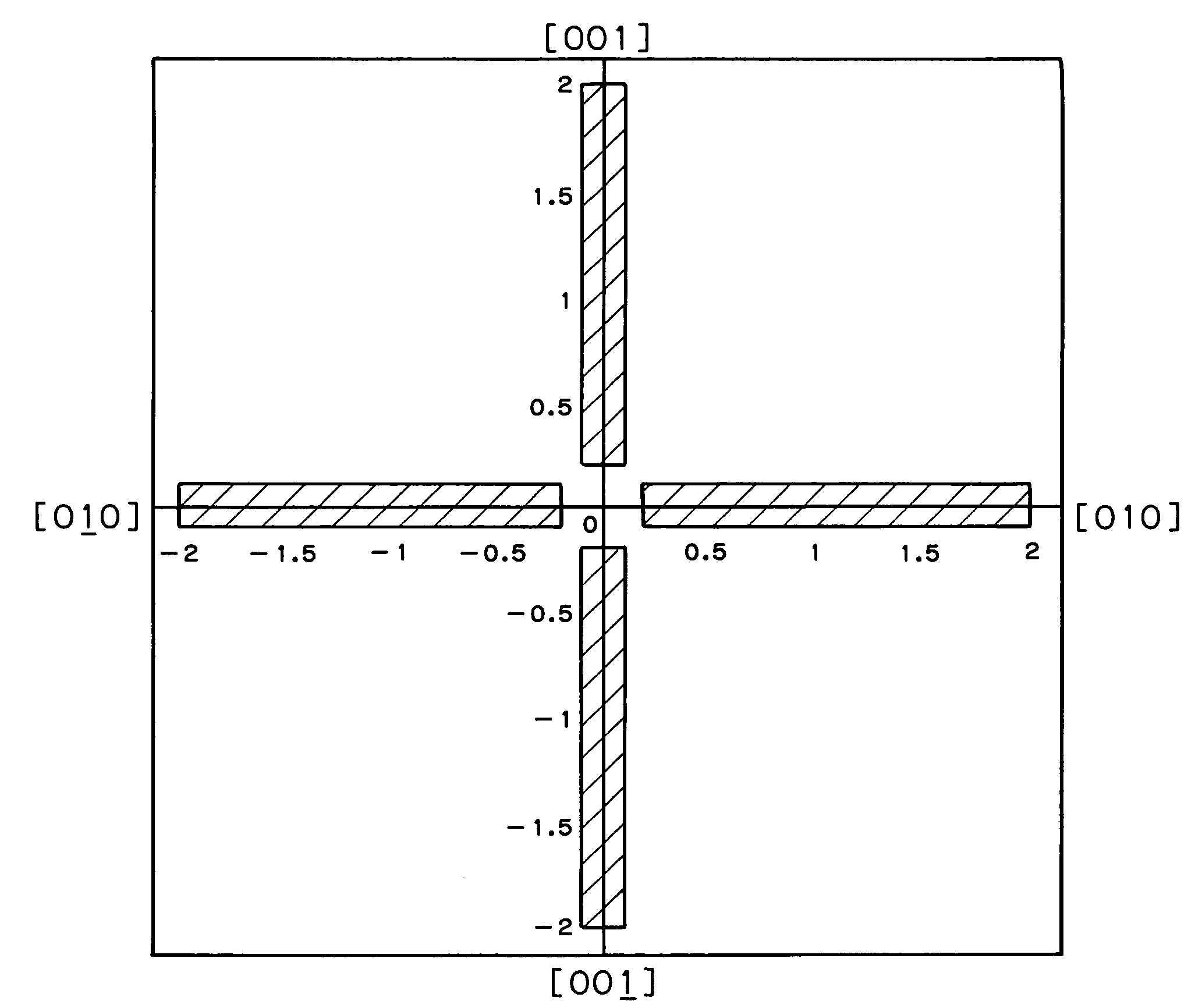
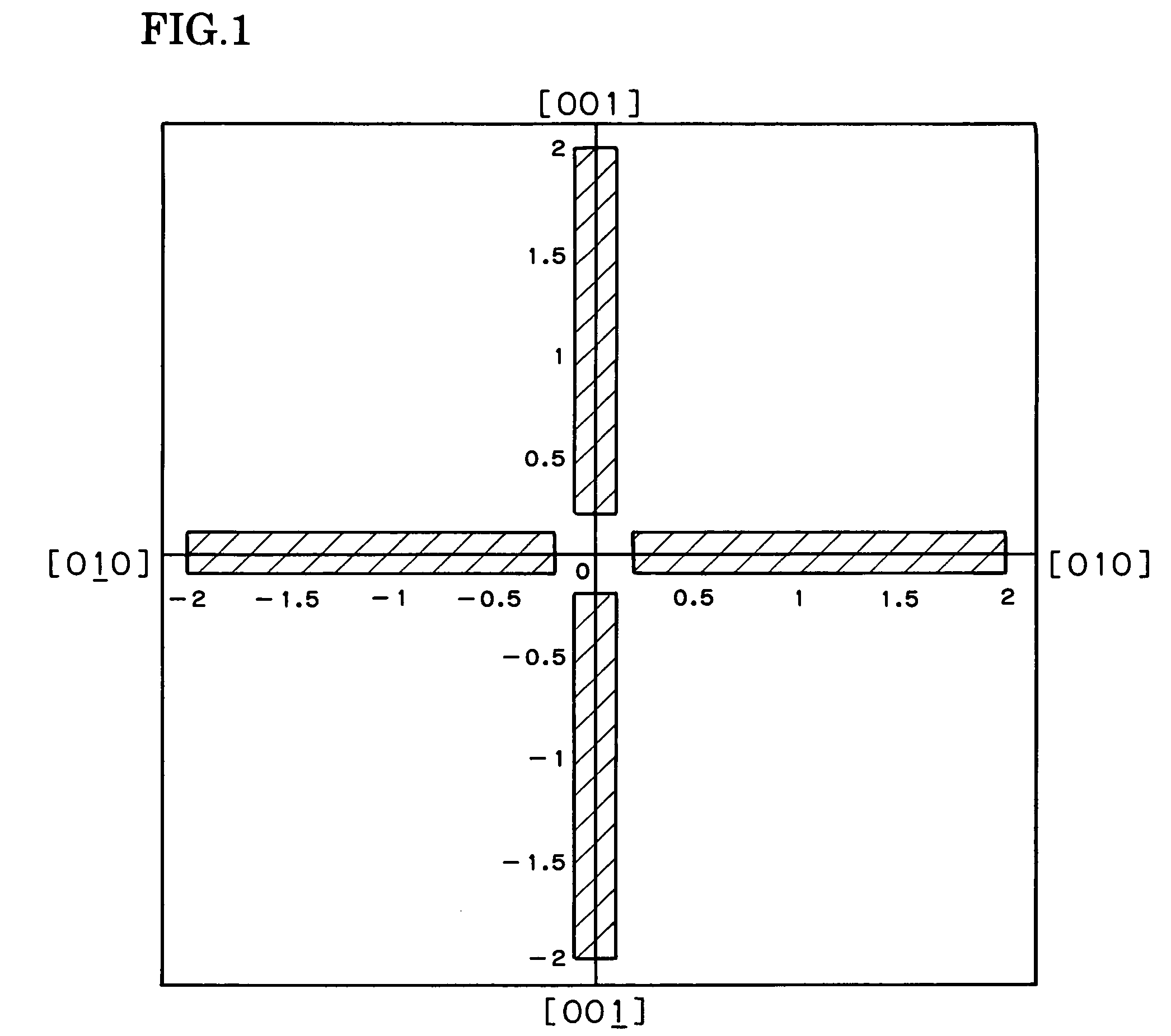
[0012]As a result of diligent research into the tilt of the crystal axis and the planar orientation of a wafer in an effort to reduce the pitting of an epitaxial layer, the inventors perfected the present invention upon discovering that a sound epitaxial layer can be obtained by specifying a tilt angle of orientation that is different from the tilt angle specified in order to improve micro-roughness or tear-drop formation in the past as discussed above.
[0014]Also, the epitaxial wafer pertaining to the present invention is characterized in that an epitaxial film is formed on a wafer surface that has undergone gas etching for the sake of cleaning prior to epitaxial film formation, which reduces the number of pits seen after epitaxial film formation.

Problems solved by technology

However, when a silicon (100) substrate wafer was epitaxially grown within these numerical ranges, the epitaxial wafer surface was sometimes rougher than the substrate wafer surface, which made it difficult to control the micro-roughness of the epitaxial wafer surface.

Method used


Image

  • Epitaxial wafer and method for manufacturing method
  • Epitaxial wafer and method for manufacturing method

Examples


example 1

[0032]Using a wire saw apparatus (made by Nippei Toyama), silicon monocrystalline wafers were produced from a silicon monocrystalline ingot that had been doped with arsenic, had an outside diameter of 6 inches, and had been pulled up by the Czochralski method. The resulting wafers had a resistivity of 4 mΩ·cm, were n-type, and the tilt angles from the (100) plane were θ=0.24° and φ=0.02°.

[0033]These wafers were mirror polished and washed, after which they were subjected to hydrogen baking in which they were held for 1 minute in a 1150° C. hydrogen atmosphere, and then HCl gas was introduced to perform gas etching to a depth of about 0.1 μm. A source gas was then supplied and vapor phase growth was performed while the temperature was held at 1100° C., which formed an epitaxial layer with a thickness of 4 μm.

[0034]In the above steps, the condition of the wafer surface was observed by light scattering method (A) prior to placing the wafer in the vapor phase growth apparatus, (B) after ...

example 2

[0037]Using a wire saw apparatus, silicon monocrystalline wafers were produced from a silicon monocrystalline ingot that had been doped with arsenic, had an outside diameter of 6 inches, and had been pulled up by the Czochralski method. The resulting wafers had a resistivity of 4.8 mΩ·cm, were n-type, and the tilt angles from the (100) plane were θ=0.20° and φ=0.10°.

[0038]An epitaxial layer with a thickness of 4 μm was formed under the same conditions as in Example 1, using the wafer obtained above. The product was observed and measured under the same conditions as in Example 1. Specifically, Table 1 shows the defect counts prior to placing the wafer in the vapor phase growth apparatus (A), after gas etching (B), and after epitaxial film formation (C).

[0039]Regarding the defect counts in Table 1, the COP count prior to placing the wafer in the vapor phase growth apparatus (A) was 25, 303, the number of pits after gas etching (B) was 2754, and the number of pits after epitaxial film ...


PUM

PropertyMeasurementUnit
resistivityaaaaaaaaaa
depthaaaaaaaaaa
temperatureaaaaaaaaaa

Abstract

It is an object of the present invention to provide an epitaxial wafer with fewer pit defects in the epitaxial layer of a silicon monocrystalline wafer that has been doped with arsenic. Pit defects tend to occur when gas etching is performed prior to epitaxial film formation, but this tendency is reversed and a sound epitaxial layer is obtained by setting the crystal plane orientation to (100) and specifying the range of the tilt angle for the angle θ in the [001] direction or [001] direction or the angle φ in the [010] direction or [010] direction with respect to the [100] axis.

Description

CROSS-REFERENCE TO PRIOR APPLICATION[0001]This is a U.S. national phase application under 35 U.S.C. § 371 of International Patent Application No. PCT / JP03 / 10390 filed Aug. 15, 2003, and claims the benefit of Japanese Patent Application No. 2002-252463 filed Aug. 30, 2002, which is incorporated by reference herein.TECHNICAL FIELD[0002]This invention relates to an epitaxial wafer with fewer pit defects in the epitaxial layer, and more particularly relates to the above-mentioned epitaxial wafer in which the number of pit defects has been reduced by using a wafer produced by slicing an ingot in a specific planar orientation, for a silicon monocrystalline wafer that has been doped with arsenic (As) and is prone to pitting when subjected to gas etching prior to epitaxial film formation, and to a method for manufacturing this epitaxial wafer.BACKGROUND ART[0003]In the past, the off-angle (that is, the tilt angle) of a (100) plane substrate in the manufacture of silicon epitaxial wafers has...

Claims


Application Information

Patent Timeline
Patent Type & Authority Patents(United States)
IPC IPC(8): H01L29/04C30B25/02C30B25/20C30B29/06C30B33/00H01L21/20H01L21/205
CPCC30B29/06C30B33/00H01L21/02381H01L21/2003H01L21/02532C30B25/20H01L21/02433
Inventor UMENO, SHIGERUMURAKAMI, SATOSHIFUJII, HIROTAKA
Owner SUMITOMO MITSUBISHI SILICON CORP
Learn More