Bias circuit for a bipolar transistor

a bias circuit and bipolar transistor technology, applied in the field of hbt mmics, can solve the problems of more prone to manufacturing drift, high current drawn from the switched reference line in all cases, and difficult to set up

Inactive Publication Date: 2007-10-30
ROKE MANOR RES LTD
View PDF16 Cites 8 Cited by
  • Summary
  • Abstract
  • Description
  • Claims
  • Application Information

AI Technical Summary

Problems solved by technology

While each of the circuits have apparently provided manufacturable solutions, the current drawn from the switched reference line is in all cases rather high.
Furthermore, several of the known solutions are very ‘interactive’, and are therefore difficult to set up for the right quiescent current, self biasing profile, linearity, temperature stability etc, and are therefore more prone to manufacturing drift.

Method used


Image

  • Bias circuit for a bipolar transistor
  • Bias circuit for a bipolar transistor
  • Bias circuit for a bipolar transistor

Examples


Embodiment Construction

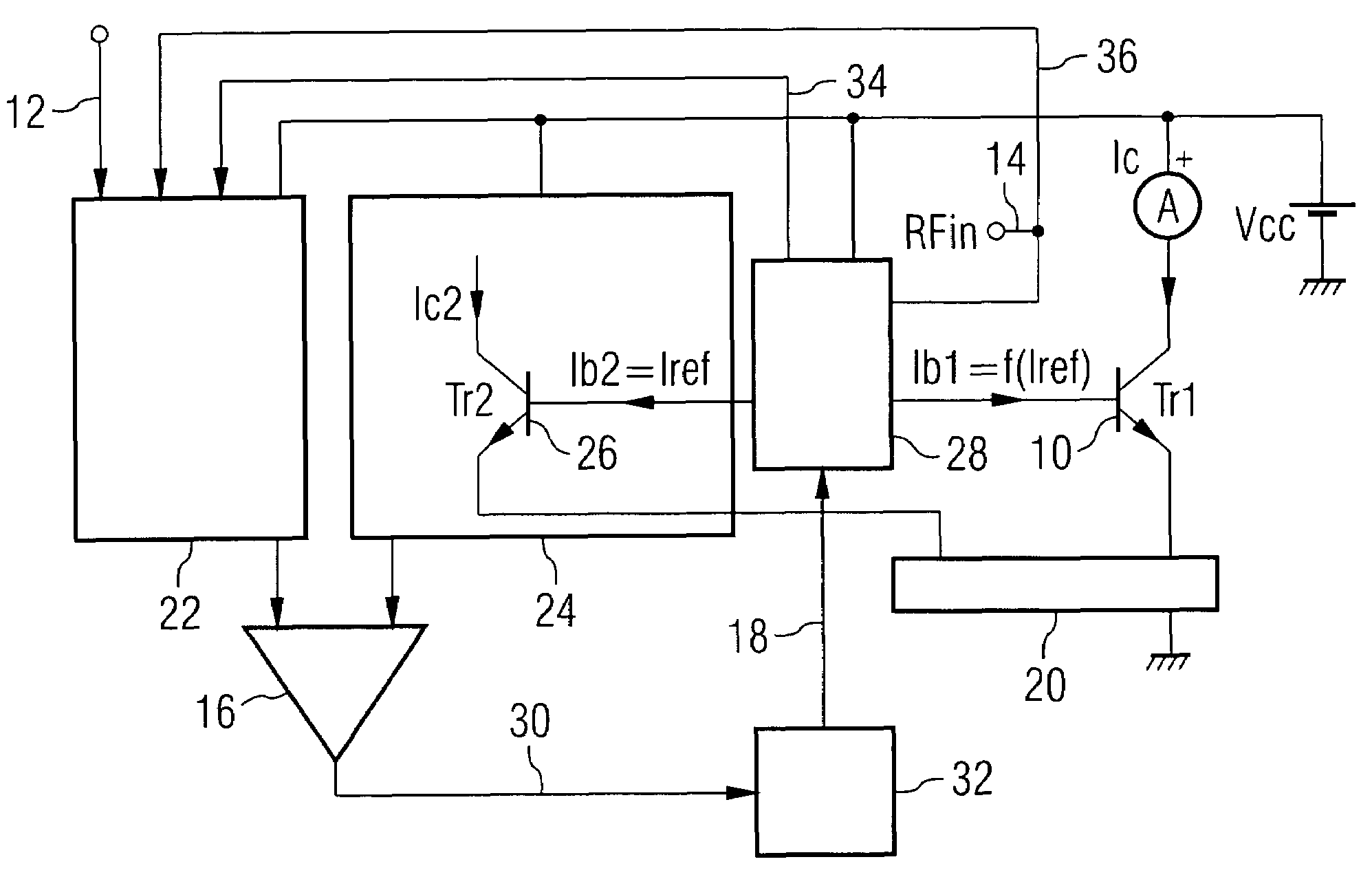
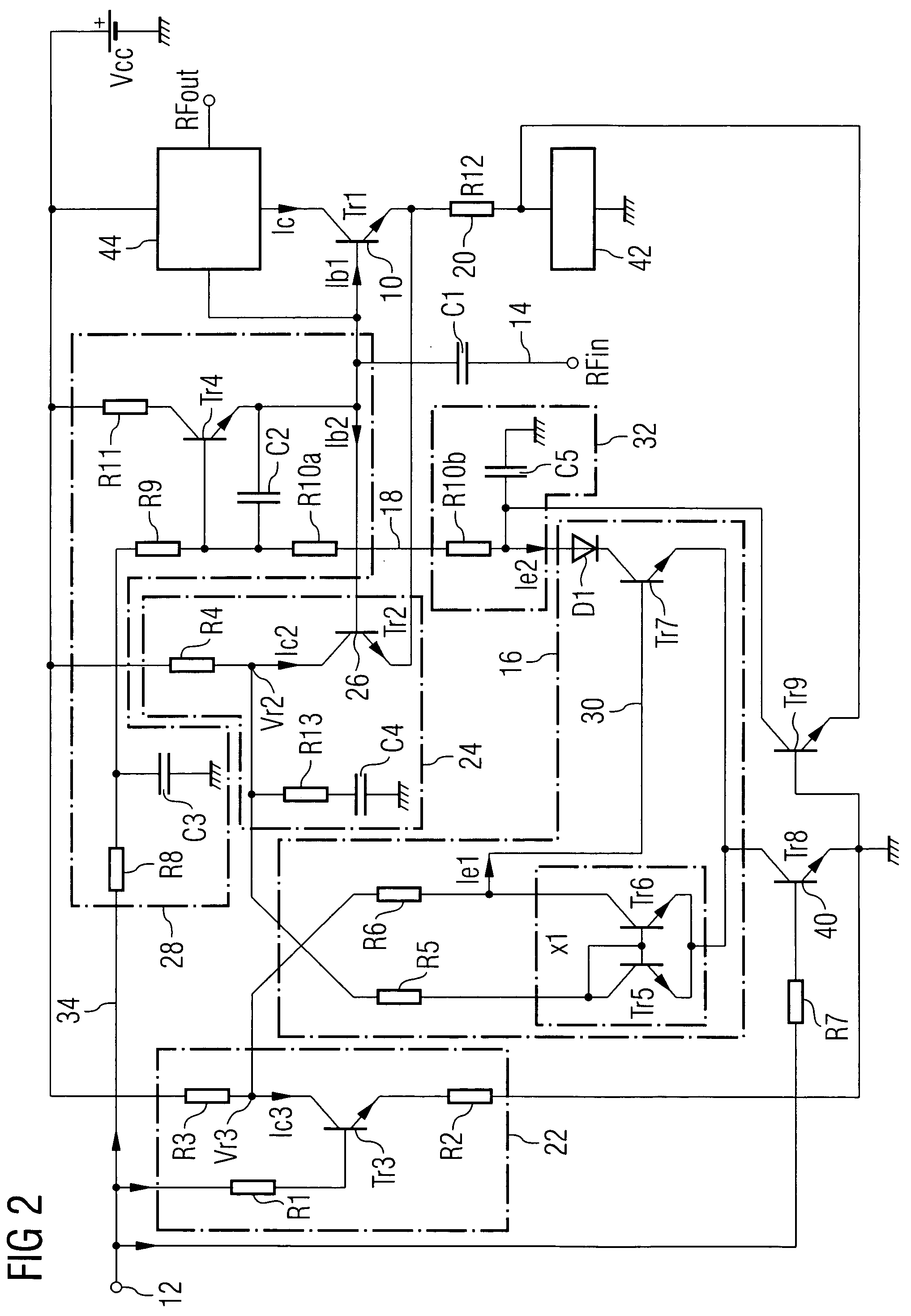
[0037]The present invention accordingly provides a transistor bias circuit which provides at least some of the following advantages:

[0038]Low control current drain from Vpd, typically 300 μA as compared to 7 mA for known circuits;[0039]excellent process tolerance: the circuit function preferably relies largely on component ratios, rather than absolute values;[0040]excellent power supply tolerance;[0041]excellent temperature tolerance;[0042]ability to control interaction with RF signals;[0043]excellent RF power level immunity, where required; and[0044]enables optimum RF performance to be obtained from the active devices.

[0045]The circuit of the present invention may be configured for circuits requiring different operation classes, from small signal Class A circuits through to deep Class AB circuits such as power amplifiers. It is especially suited to circuits using a bipolar process with a high base-emitter junction voltage (Vbe) relative to the supply voltage (Vcc), such as HBT MMIC...


PUM


Abstract

The bias circuit of the present invention can be configured for extremely stiff biasing for Class A circuits, which is solid under heavy RF input overdrive. Alternatively, the circuit may be configured for controlled self biasing for use in Class AB designs.

Description

[0001]The present invention relates to a bias circuit for a bipolar transistor. In particular, the invention relates to a bias circuit topology for radio frequency and microwave based bipolar amplification and function circuits.BACKGROUND OF THE INVENTION [0002]The present invention has particular application to HBT MMICs (hetero-junction bipolar transistor monolithic microwave integrated circuits). An HBT MMIC is an integrated circuit using bipolar transistors, suitable for generation of relatively high radio frequency power levels. The present invention finds application in the transmitter path of a mobile phone handset. It is particularly suited to applications using linear modulation, such as the CDMA and W-CDMA schemes, as used in the emerging UMTS market.[0003]HBT MMIC integrated circuits likely to be required in the transmit path of a handset include Driver Amplifiers, Variable Gain Amplifiers (VGA), and Power Amplifiers (PA).[0004]Optimal RF performance of an HBT MMIC can on...

Claims


Application Information

Patent Timeline
Patent Type & Authority Patents(United States)
IPC IPC(8): H03F3/04H03C1/36H03F1/02H03F1/30
CPCH03C1/36H03F1/0266H03F1/302H03F3/19H03F2200/75H03F2200/18H03F2200/222
Inventor BIRKBECK, JOHN DAVID
Owner ROKE MANOR RES LTD
Why Eureka
Try Eureka