

Universal modular wafer transport system
- Summary
- Abstract
- Description
- Claims
- Application Information
AI Technical Summary
Benefits of technology
Problems solved by technology
Method used
Image

Examples
Embodiment Construction
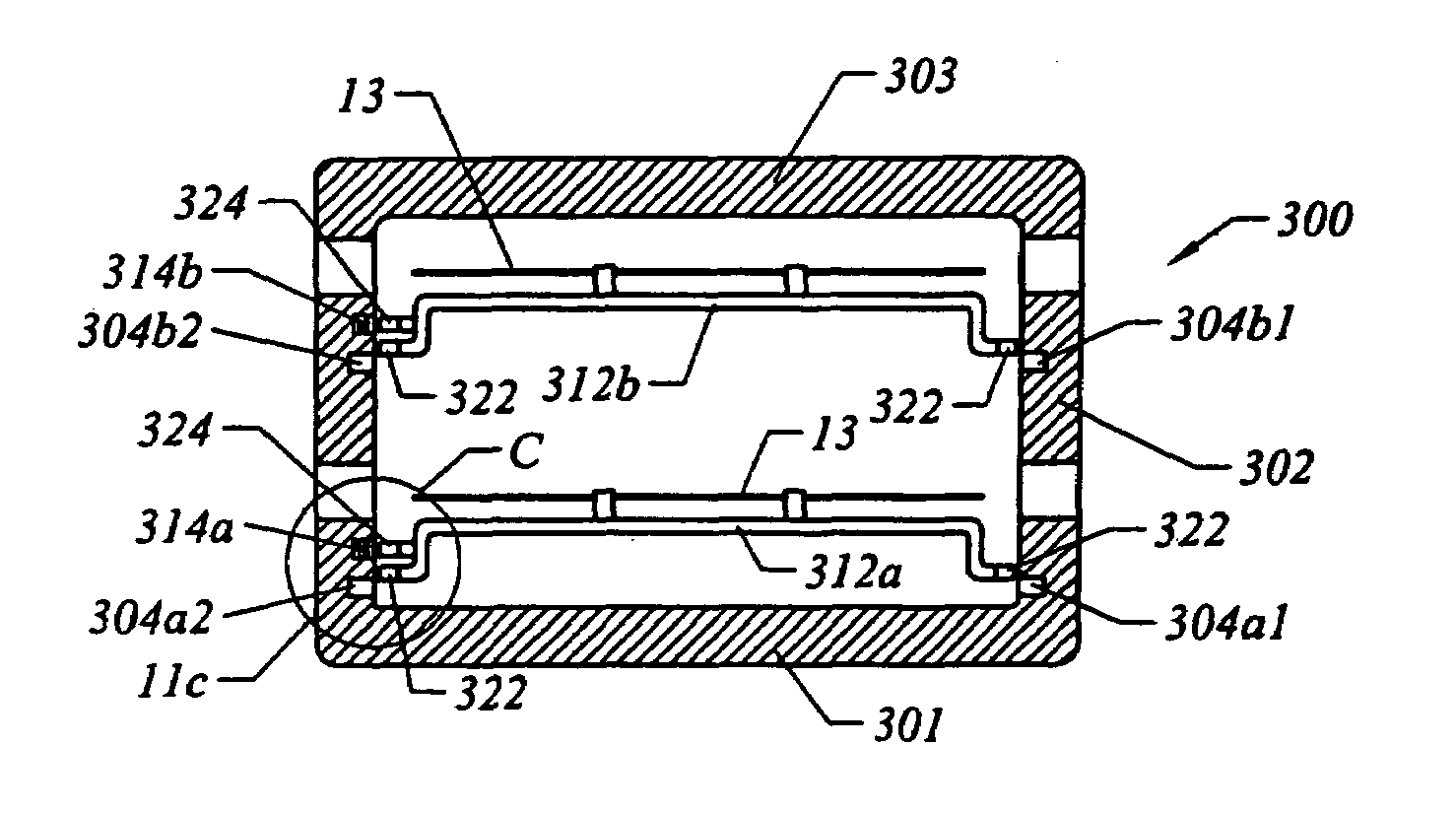
[0045]The wafer transfer system 100 is an architectural approach to constructing a tool-to-tool wafer transport system. As described in more detail below, a preferred embodiment of the wafer transfer system 100 transports individual wafers within an isolated environment. Other embodiments of the wafer transfer system 100 may transport multiple wafers, a packet of wafers, or a wafer cassette between processing stations.
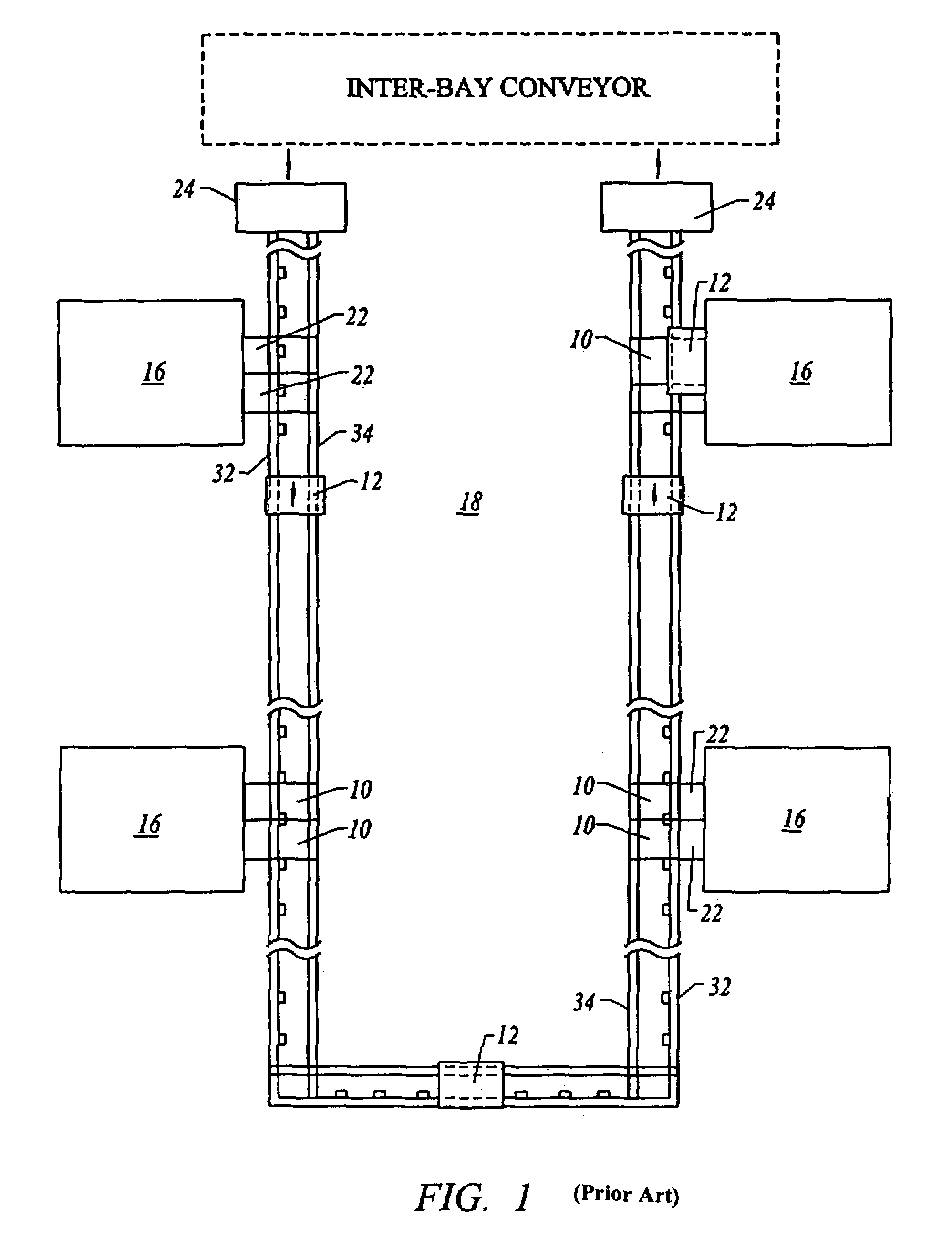
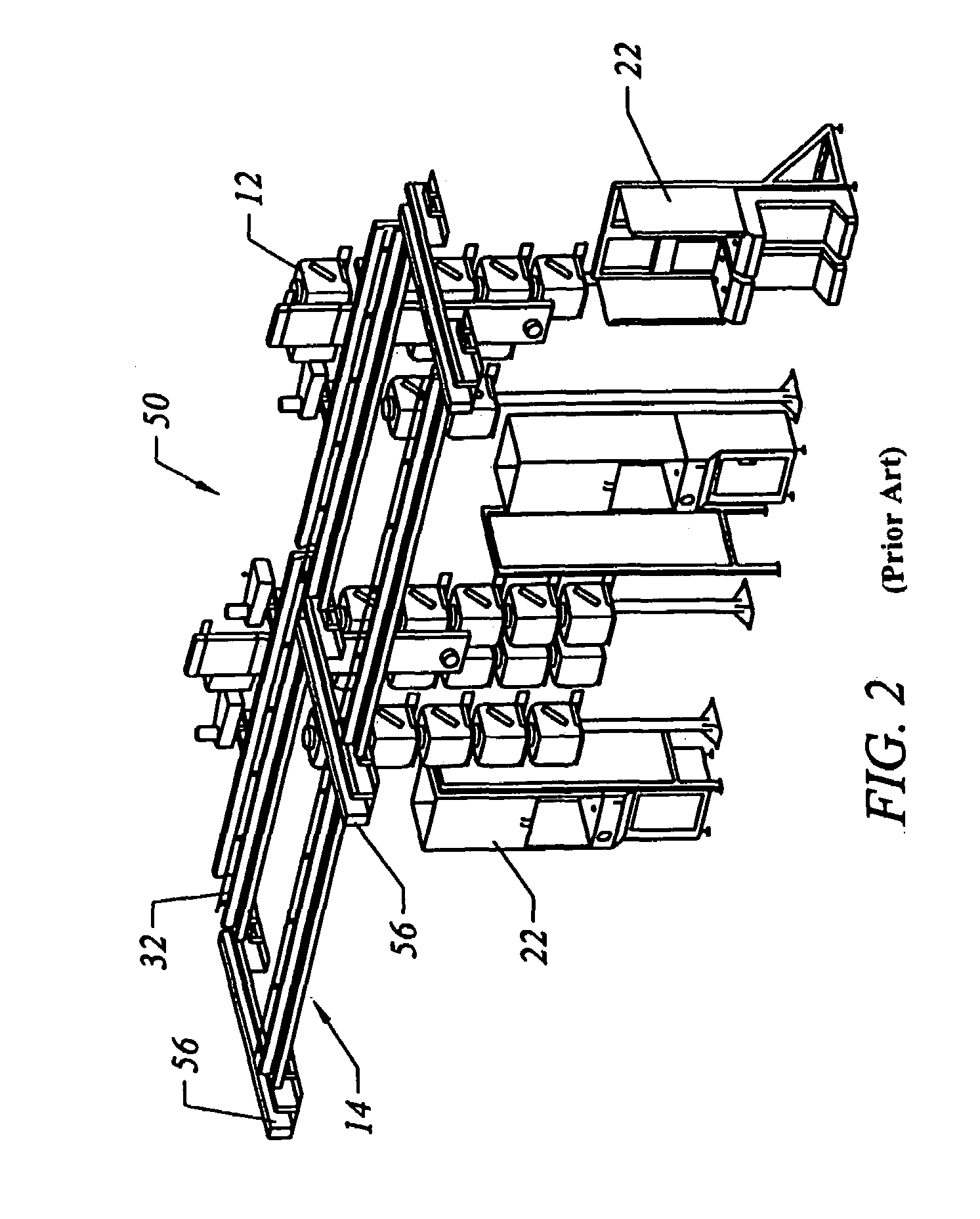
[0046]FIG. 4 illustrates a first embodiment of the wafer transfer system 100. In general, the wafer transport system 100 is designed to transport a wafer 13 initially from an EFEM 22, and then between chambers 16—not returning the wafer 13 to the EFEM 22 until the process sequence is complete. The wafer transport enclosure 102 provides an isolated, clean environment to execute all of these tasks. As shown in FIG. 4, a first embodiment of the wafer transport enclosure 102 includes at least one wafer transport tube 104, and a transition chamber 108 that secures to each c...
PUM
 Abstract
Description
Claims
Application Information