
Fabrication and activation processes for nanostructure composite field emission cathodes

a technology of composite field emission cathodes and activation processes, which is applied in the manufacture of electrodialysis, isotope separation, and electrodialysis. it can solve the problems of limited practical utilization, inability to directly use devices without further processing, and generally not having the same level of structural perfection of cvd grown carbon nanotubes. achieve better adhesion and electrical conductivity

Active Publication Date: 2007-11-13
NURAY TECH
View PDF11 Cites 21 Cited by
  • Summary
  • Abstract
  • Description
  • Claims
  • Application Information

AI Technical Summary

Benefits of technology

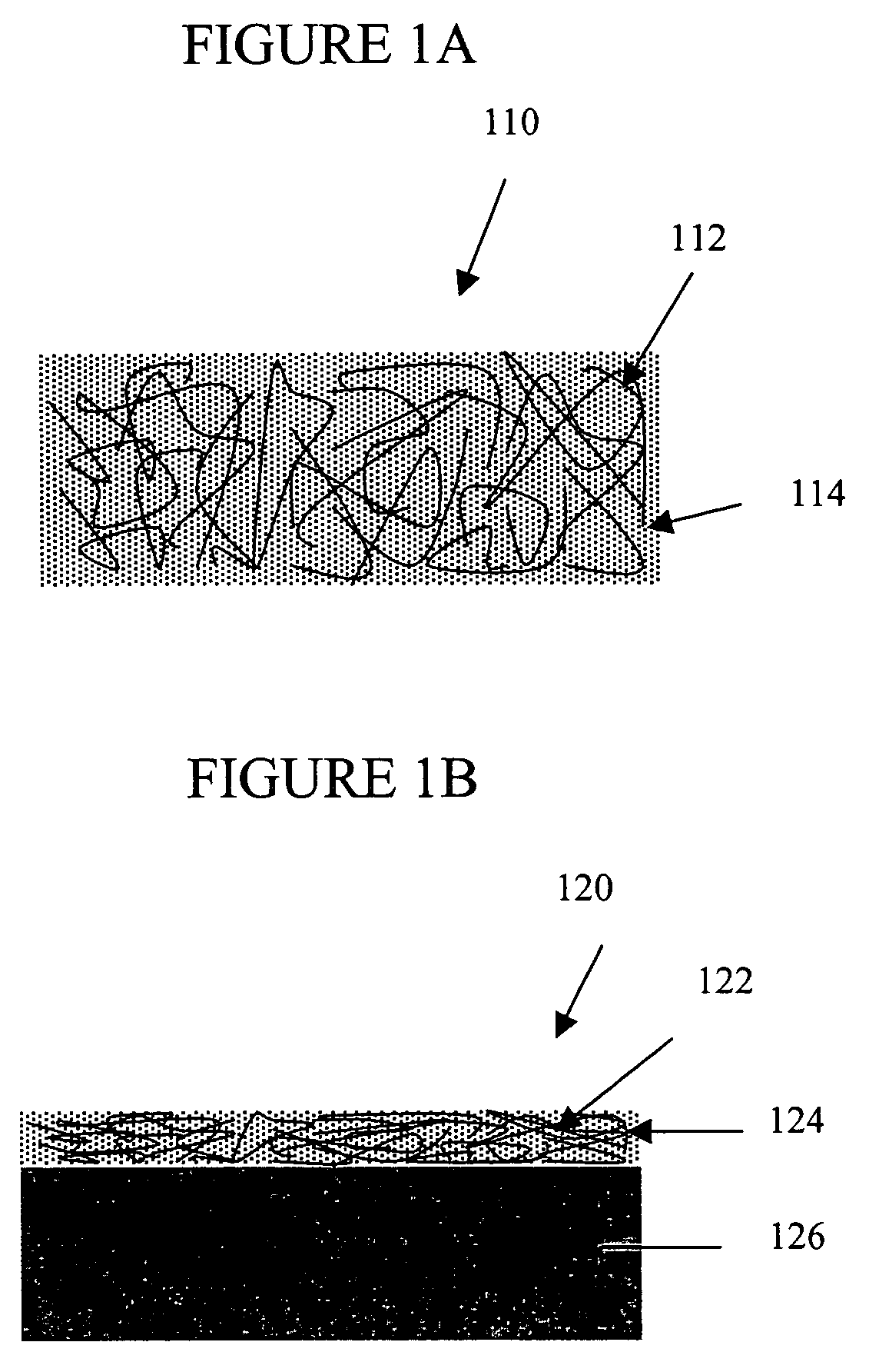
[0022]Compared with thin carbon nanotube films, a coating formed as described above provides better adhesion and electrical conductivity between the nanostructure-containing material and the substrate.

Problems solved by technology

However, due to materials issues such as poor film uniformity and insufficient adhesion and electrical conductivity between carbon nanotubes and the substrate, high stable emission current has not been obtained from macroscopic carbon nanotube-containing structures and devices, which has limited their practical utilization.
However, materials made therefrom are in the form of either porous membranes or powders that are not easily incorporated into field-emission devices such as cathodes, and therefore cannot be used directly on devices without further processing.
Also, CVD grown carbon nanotubes generally do not have the same level of structural perfection and, as a result, lack the same emission properties as the tubes made by laser-ablation or arc-discharge methods.
Thus, the normal lack of orientation of the nanotubes presents and additional challenge to their utilization in field-emission devices.

Method used


Image

  • Fabrication and activation processes for nanostructure composite field emission cathodes
  • Fabrication and activation processes for nanostructure composite field emission cathodes
  • Fabrication and activation processes for nanostructure composite field emission cathodes

Examples


Embodiment Construction

[0030]Exemplary arrangements and techniques according to the present invention will now be described by reference to the drawing figures.

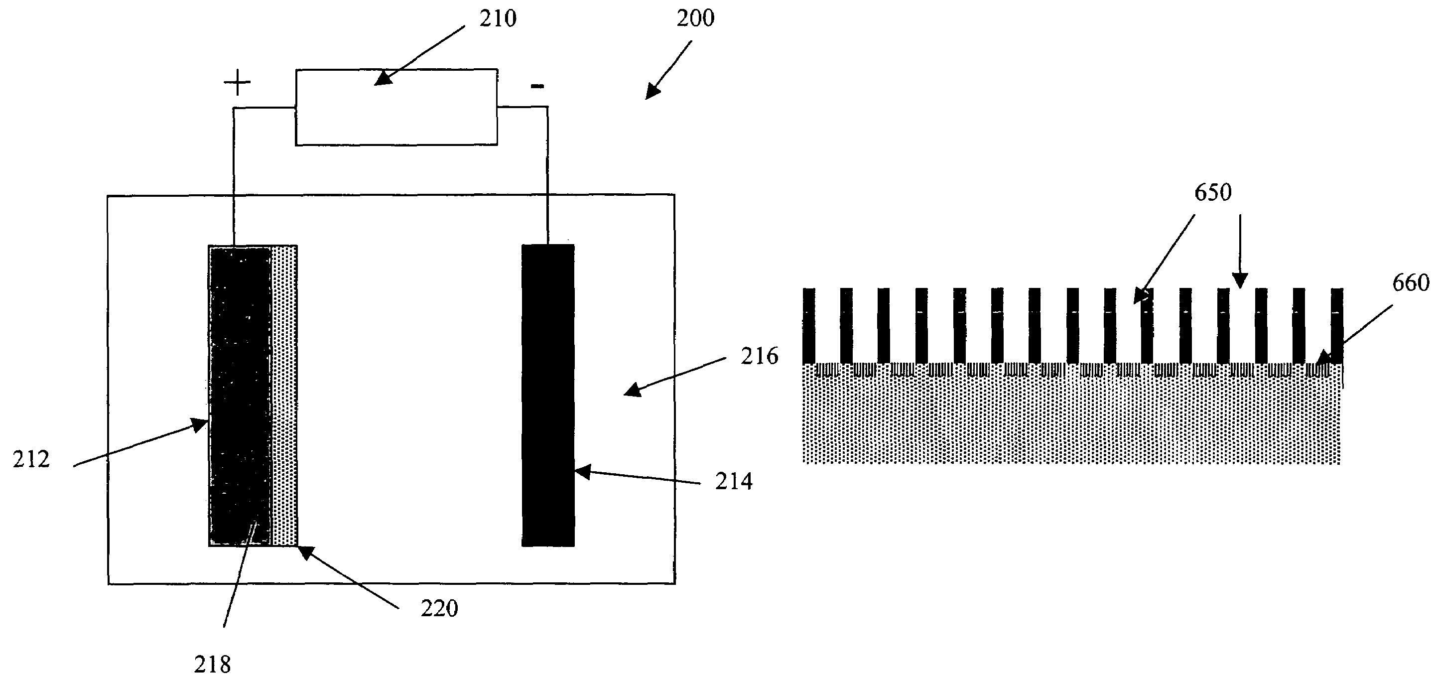
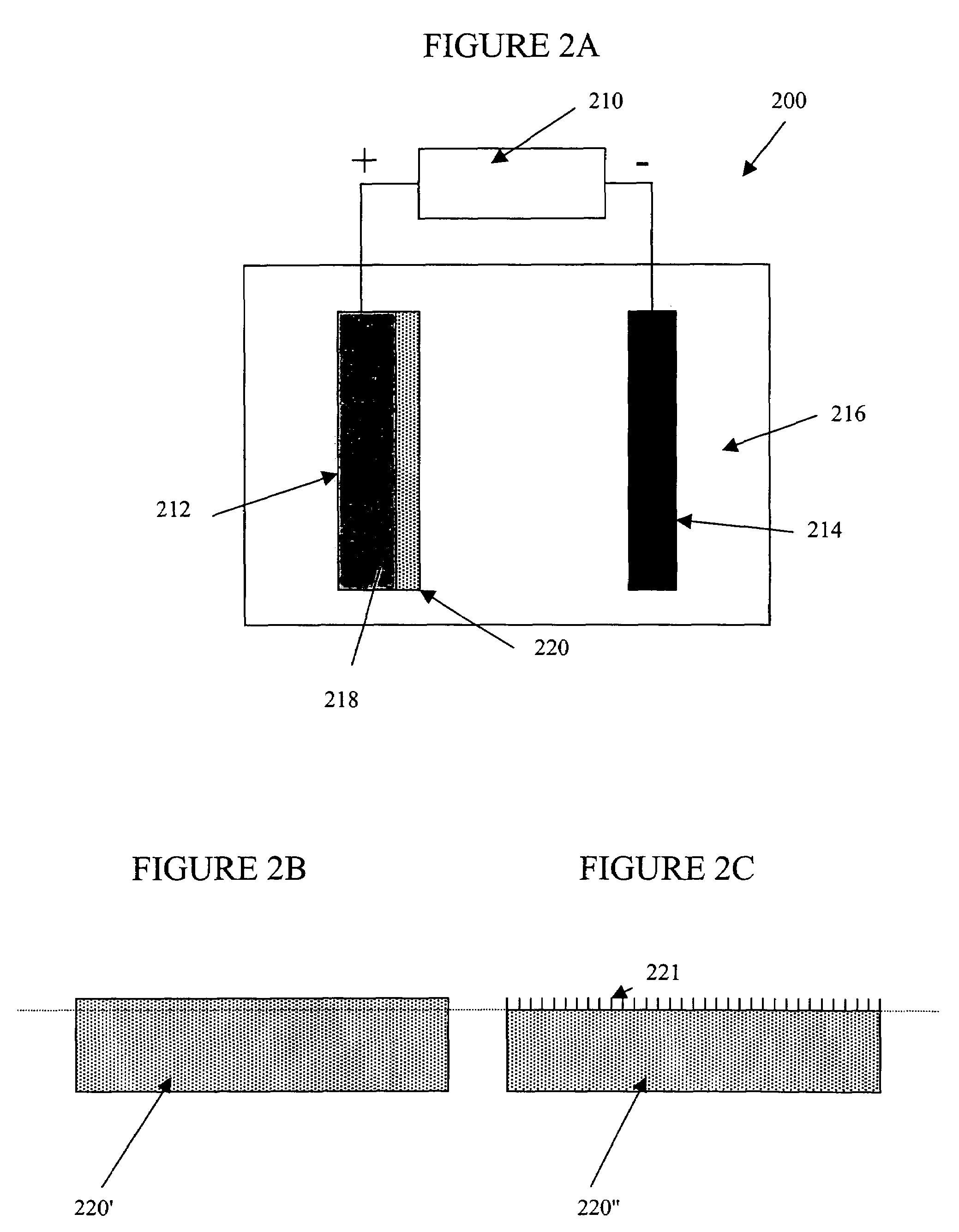
[0031]Generally, a method performed according to the principles of the present invention can include a combination of some or all of the following steps: (1) forming a raw nanostructure-containing material by a suitable technique, such as arc-discharge or laser ablation; (2) forming a mixture of nanostructure-containing material and a matrix material; (3) applying the mixture to a supporting surface or substrate, or forming the mixture into a free-standing body; (4) pressing the mixture to improve surface uniformity and / or flatness; (5) sintering or melting the mixture; (6) polishing and rinsing the sintered mixture; (6) etching the sintered mixture to remove matrix material and expose nanostructure material; (7) rinsing the etched mixture; (8) annealing the etched mixture; and (9) aligning the nanostructure material exposed by the etching procedur...


PUM

PropertyMeasurementUnit
Temperatureaaaaaaaaaa
Lengthaaaaaaaaaa

Abstract

A method of forming an electron emitter includes the steps of: (i) forming a nanostructure-containing material; (ii) forming a mixture of nanostructure-containing material and a matrix material; (iii) depositing a layer of the mixture onto at least a portion of at least one surface of a substrate by electrophoretic deposition; (iv) sintering or melting the layer thereby forming a composite; and (v) electrochemically etching the composite to remove matrix material from a surface thereof, thereby exposing nanostructure-containing material.

Description

[0001]This application claims priority under 35 U.S.C. 119 to U.S. Provisional Application No. 60 / 393,097 entitled “Fabrication and Activation Processes of Field Emission Cathodes Composed of Carbon Nanotubes / Metal Composites”, and filed on Jul. 3, 2002, the entire content of which is incorporated herein by referenceFIELD OF THE INVENTION[0002]The present invention is directed to improved techniques for the formation field emission structures and devices that incorporate nanostructure-containing material, as well as treatments to improve the performance thereof. The present invention is also directed to associated structures and devices.BACKGROUND OF THE INVENTION[0003]Various constructions and techniques will be described below. However, nothing described herein should be construed as an admission of prior art. To the contrary, Applicants expressly reserve the right to demonstrate, where appropriate, that anything described herein does not qualify as prior art under the applicable ...

Claims


Application Information

Patent Timeline
IPC IPC(8): C25D13/02C25F3/02H01J9/02
CPCB82Y10/00C25D5/48H01J9/025C25D15/02H01J2201/30469
Inventor GAO, BO
Owner NURAY TECH
Learn More