Method for controlling poly 1 thickness and uniformity in a memory array fabrication process

a memory array and fabrication process technology, applied in semiconductor/solid-state device manufacturing, basic electric elements, electric devices, etc., can solve the problems of undesirable non-uniformity, difficult to achieve accurate final thickness of poly 1 segments, and unsatisfactory core erosion without providing good stopping capability, so as to avoid undesirable non-uniformity and core erosion

Active Publication Date: 2007-11-13
CYPRESS SEMICON CORP
View PDF3 Cites 0 Cited by
  • Summary
  • Abstract
  • Description
  • Claims
  • Application Information

AI Technical Summary

Benefits of technology

[0006]The present invention is directed to method for controlling poly 1 thickness and uniformity in a memory array fabrication process. The present invention addresses and resolves the need in the art for a me

Problems solved by technology

However, the CMP “over-polish” process causes undesirable core erosion without providing good stopping capability.
As a result, an accurate final thickness of poly 1 segments is difficult to achieve

Method used


Image

  • Method for controlling poly 1 thickness and uniformity in a memory array fabrication process
  • Method for controlling poly 1 thickness and uniformity in a memory array fabrication process
  • Method for controlling poly 1 thickness and uniformity in a memory array fabrication process

Examples


Embodiment Construction

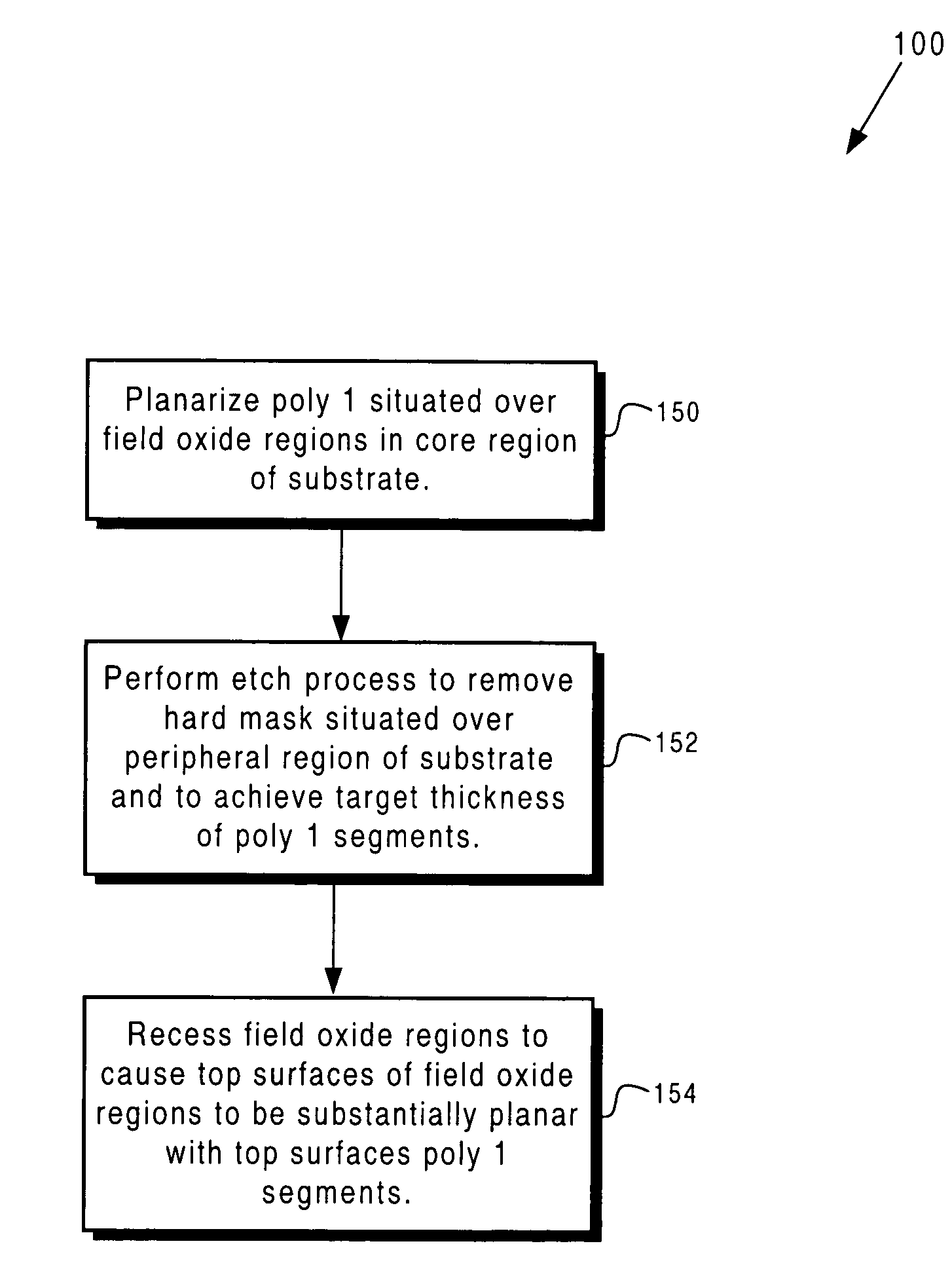
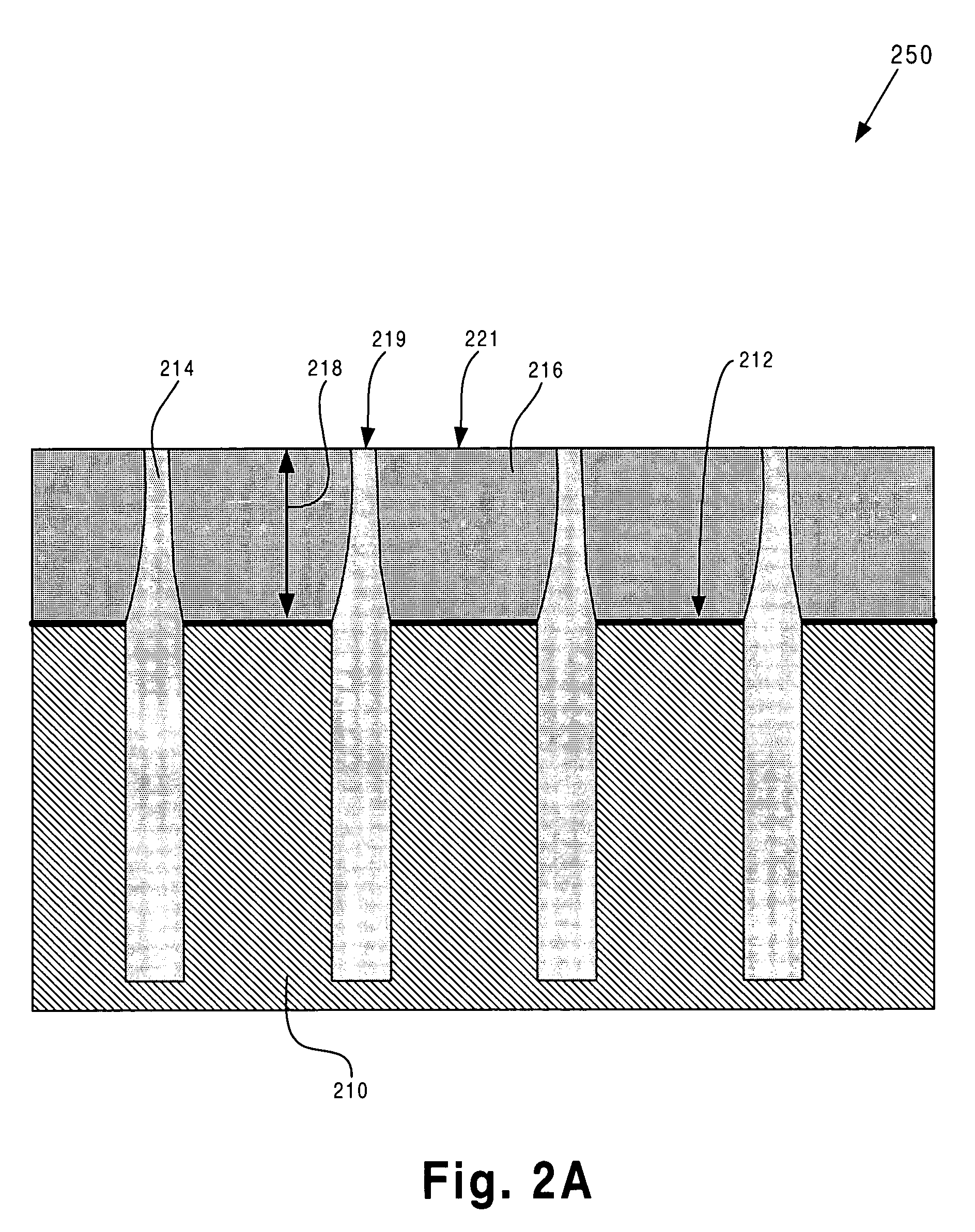
[0014]The present invention is directed to method for controlling poly 1 thickness and uniformity in a memory array fabrication process. The following description contains specific information pertaining to the implementation of the present invention. One skilled in the art will recognize that the present invention may be implemented in a manner different from that specifically discussed in the present application. Moreover, some of the specific details of the invention are not discussed in order not to obscure the invention.

[0015]The drawings in the present application and their accompanying detailed description are directed to merely exemplary embodiments of the invention. To maintain brevity, other embodiments of the present invention are not specifically described in the present application and are not specifically illustrated by the present drawings. It should be borne in mind that, unless noted otherwise, like or corresponding elements among the figures may be indicated by lik...


PUM


Abstract

According to one exemplary embodiment, a method includes planarizing a layer of polysilicon situated over field oxide regions on a substrate to form polysilicon segments, where the polysilicon segments have top surfaces that are substantially planar with top surfaces of the field oxide regions, and where the field oxide regions have a first height and the polysilicon segments have a first thickness. The method further includes removing a hard mask over a peripheral region of the substrate. According to this exemplary embodiment, the method further includes etching the polysilicon segments to cause the polysilicon segments to have a second thickness, which causes the top surfaces of the polysilicon segments to be situated below the top surfaces of the field oxide regions. The polysilicon segments can be etched by using a wet etch process. The polysilicon segments are situated in a core region of the substrate.

Description

TECHNICAL FIELD[0001]The present invention is generally in the field of semiconductor devices. More particularly, the present invention is in the field of fabrication of memory arrays.BACKGROUND ART[0002]Conventional memory array, such a flash memory array, typically includes one or more high-density core regions and a low-density periphery region on a single substrate. Memory transistors in the core have a substantially similar stacked gate structure. The stacked gate structure includes a floating gate comprising a first layer of polysilicon (poly 1) underneath a control gate. The control gate comprises a second layer of polysilicon (poly 2).[0003]Processing steps for fabricating a memory array, such as a flash memory array, include, among other steps, forming a gate oxide layer and isolation regions in core and peripheral regions of a substrate. Poly 1 is deposited over the gate oxide layer and the isolation regions and a chemical mechanical polish (“CMP”) process is typically use...

Claims


Application Information

Patent Timeline
IPC IPC(8): H01L21/302H01L21/461
CPCH01L21/7684
Inventor ACHUTHAN, KRISHNASHREEKIM, UNSOONSAHOTA, KASHMIRREGALADO, PATRIZ C.
Owner CYPRESS SEMICON CORP
Why Eureka
Try Eureka