Miniaturized, low power fgmosfet radiation sensor and wireless dosimeter system

a radiation sensor and wireless technology, applied in the field of low-power fgmosfet radiation sensors and dosimeters, can solve the problems of increasing sensitivity and reducing capacitan

Active Publication Date: 2010-04-22
KING ABDULLAH UNIV OF SCI & TECH
View PDF8 Cites 40 Cited by
  • Summary
  • Abstract
  • Description
  • Claims
  • Application Information

AI Technical Summary

Benefits of technology

[0013]Elimination of a conventional control gate, and provision of a charge injector structure in the substrate, rather than a conventional charge injector gate over the floating gate, reduces capacitance and increases sensitivity. The substrate charge injector is isolated by a gate oxide layer from the floating gate and allows for pre-charging by electron tunneling. The charge injector may take the form of a shorted MOS transistor in the adjacent substrate underlying part of the floating gate. This structure can therefore be fabricated using a single polysilicon CMOS process. Since there is no control gate, the radiation dose may be monitored by applying a small bias, e.g. ˜0.1V applied to the drain terminal, to monitor the channel current or drain current ID.
[0020]In preferred embodiments, sensitivity was observed to be improved by about 10% when the capacitance to the floating gate is reduced by eliminating a conventional charging gate on top of the floating gate, and using elevated metal shielding to allow for a thicker dielectric layer underneath the shielding electrode. Both the enhanced sensitivity and presence of an identical FG reference MOSFET permit lower voltage operation.
[0027]Thus, embodiments of the invention provide a miniaturized, sensitive and reliable low power radiation sensor, which may be fabricated in standard low-cost CMOS technology, which may be more readily integrated monolithically with signal processing circuitry, and coupled with a wireless transmitter.

Problems solved by technology

Elimination of a conventional control gate, and provision of a charge injector structure in the substrate, rather than a conventional charge injector gate over the floating gate, reduces capacitance and increases sensitivity.

Method used


Image

  • Miniaturized, low power fgmosfet radiation sensor and wireless dosimeter system
  • Miniaturized, low power fgmosfet radiation sensor and wireless dosimeter system
  • Miniaturized, low power fgmosfet radiation sensor and wireless dosimeter system

Examples


first embodiment

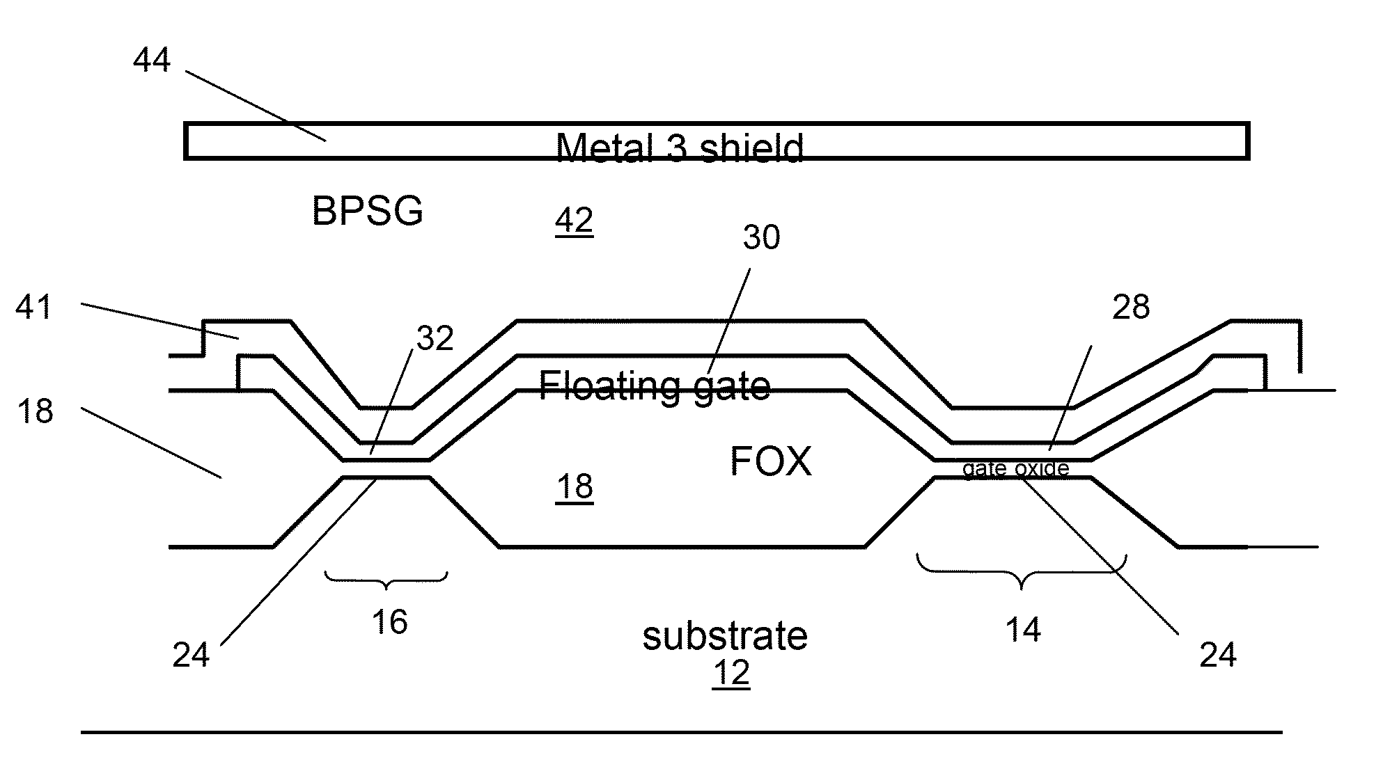
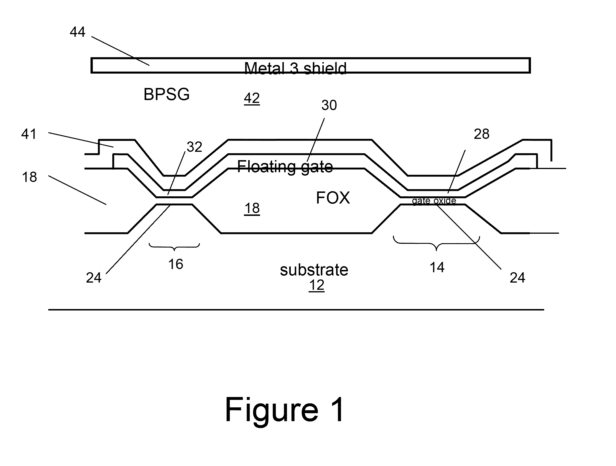
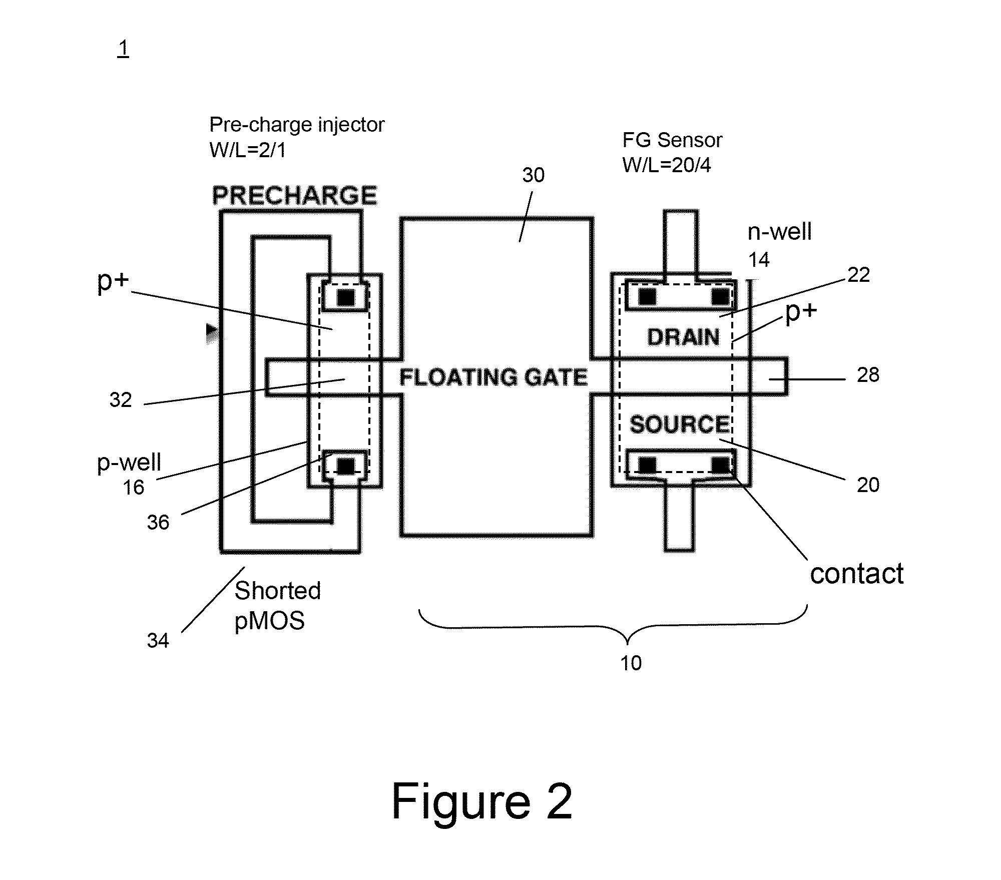
[0043]A radiation sensor 1 comprising a FGMOSFET 10 according to the present invention is shown schematically in cross-section in FIG. 1. A top view of part of the layout is shown in FIG. 2. The exemplary device structure 1 may be fabricated using a standard 0.8 μm CMOS process (DALSA) with a single polysilicon layer. The FGMOSFET comprises a p-channel device fabricated on a silicon substrate 12, in which a first device well region (n-well) 14 and a second device well region (p-well) 16 are defined, separated by field oxide regions (FOX) 18. As shown in FIG. 2, source 20, drain 22 and channel 24 regions of the sensor FGMOSFET 10 are defined in the substrate in the first device well 14. A standard thickness gate oxide layer 24 is provided over the channel region and a floating gate 28 is formed thereon, comprising a polysilicon layer (Poly 1). The floating gate 28 also comprises a larger area extension 30, provided by the first polysilicon layer, which extends over the field oxide la...

third embodiment

[0050]A sensor, is shown in FIG. 6, which shows A) a photomicrograph and B) a schematic layout of a radiation sensor comprising a FGMOSFET pair that are similar to those shown in FIG. 4, but wherein the sources, drains and gates, other than the large area floating gate extension 30, of the sensor and reference FGMOSFETS, comprise an interdigitated structure 70 to more effectively neutralize gradient effects and temperature variations across the chip. Each has a charging structure or charge injector 34, as described above. This embodiment provides for improved matching of component values to compensate for environmental and process variations, particularly for differential operation. The design provided improved accuracy, precision and a lower resolvable radiation sensitivity, because common mode variation was filtered out more effectively and improves signal to noise ratio. However, sensitivity was observed to be slightly reduced relative to the embodiment shown in FIGS. 4 and 5.

fourth embodiment

[0051]A sensor, is shown in FIG. 6 which shows A) a photomicrograph and B) a schematic layout of a FGMOSFET sensor comprising two pairs of sensor and reference FGMOSFETs 10a / 50a and 10b / 50b connected in parallel. Stacking of multiple sensors improves the sensitivity linearly with the number of stacked units. For example, the device shown in FIG. 6 with two sensor / reference FGMOSFET pairs in parallel, had an effective sensitivity of 15.1 nA / rad (3 mV / rad) compared with 7.75 nA / rad (1.5 mV / rad) for a single sensor / reference FGMOSFET pair shown in FIGS. 4 and 5. At the same time, 1 / f noise of the individual units will accumulate, which increases the minimum level of resolvable dose.

[0052]In addition to radiation sensitivity, i.e. change in threshold voltage Vt relative to the radiation dose in rads, measured in mV / rad, other important RADFET parameters are long term-fading and endurance, read-time stability, flicker (1 / f) noise and resolution. In the embodiments described herein, flic...


PUM


Abstract

A miniaturized floating gate (FG) MOSFET radiation sensor system is disclosed, The sensor preferably comprises a matched pair of sensor and reference FGMOSFETs wherein the sensor FGMOSFET has a larger area floating gate with an extension over a field oxide layer, for accumulation of charge and increased sensitivity. Elimination of a conventional control gate and injector gate reduces capacitance, and increases sensitivity, and allows for fabrication using standard low cost CMOS technology. A sensor system may be provided with integrated signal processing electronics, for monitoring a change in differential channel current ID, indicative of radiation dose, and an integrated negative bias generator for automatic pre-charging from a low voltage power source. Optionally, the system may be coupled to a wireless transmitter. A compact wireless sensor System on Package solution is presented, suitable for dosimetry for radiotherapy or other biomedical applications.

Description

CROSS REFERENCE TO RELATED APPLICATIONS [0001]This application claims priority from U.S. provisional application Ser. No. 61 / 105,921, entitled “Miniature Wearable Wireless Biomedical Sensor System”, filed 16 Oct. 2008, which is incorporated herein by reference.FIELD OF THE INVENTION[0002]This invention relates to low power FGMOSFET sensor systems, and particularly to FGMOSFET radiation sensors and dosimeters for biomedical applications.BACKGROUND OF THE INVENTION[0003]IGFETs (insulated gate field effect transistors) may be used as sensors for detection of radiation by detecting a shift in threshold voltage (Vth) or other operating parameter after irradiation. On exposure to radiation, electron hole pairs are generated, and charge is trapped in an insulating layer of the device, e.g. a gate oxide, causing a change in electrical characteristics. Radiation detecting IGFETs, and more particularly silicon MOSFET (metal oxide semiconductor field effect transistor) devices for detection of...

Claims


Application Information

Patent Timeline
Patent Type & Authority Applications(United States)
IPC IPC(8): G01T1/02H01L27/14G01T1/26
CPCH01L27/14659G01T1/026
Inventor ARSALAN, MUHAMMADSHAMIM, ATIFTARR, NICHOLAS GARRYROY, LANGIS
Owner KING ABDULLAH UNIV OF SCI & TECH
Why Eureka
Try Eureka