High switching speed two mask schottky diode with high field breakdown

a diode and high switching speed technology, applied in the direction of semiconductor devices, semiconductor/solid-state device details, electrical apparatus, etc., can solve the problems of doubtful capability to prohibit premature breakdown and not disclose the fabricating method of the forgoing device in the chang area, so as to enhance the reverse breakdown voltage and minimize current leakage

Inactive Publication Date: 2007-12-20
CHIP INTEGRATION TECH +1
View PDF5 Cites 43 Cited by
  • Summary
  • Abstract
  • Description
  • Claims
  • Application Information

AI Technical Summary

Benefits of technology

[0009]The present invention also provides two modified methods based on the first preferred embodiment. In the second preferred embodiment, the power rectifier includes an extra n doping region formed beneath the

Problems solved by technology

Chang does not disclose fabricating method of about the forgoing devices.
Apart from that, no termination structure is include, and the capability of abou

Method used


Image

  • High switching speed two mask schottky diode with high field breakdown
  • High switching speed two mask schottky diode with high field breakdown
  • High switching speed two mask schottky diode with high field breakdown

Examples


Embodiment Construction

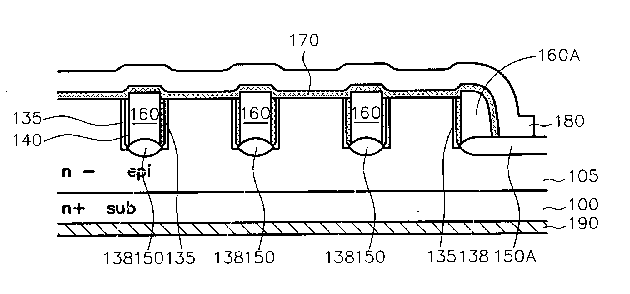
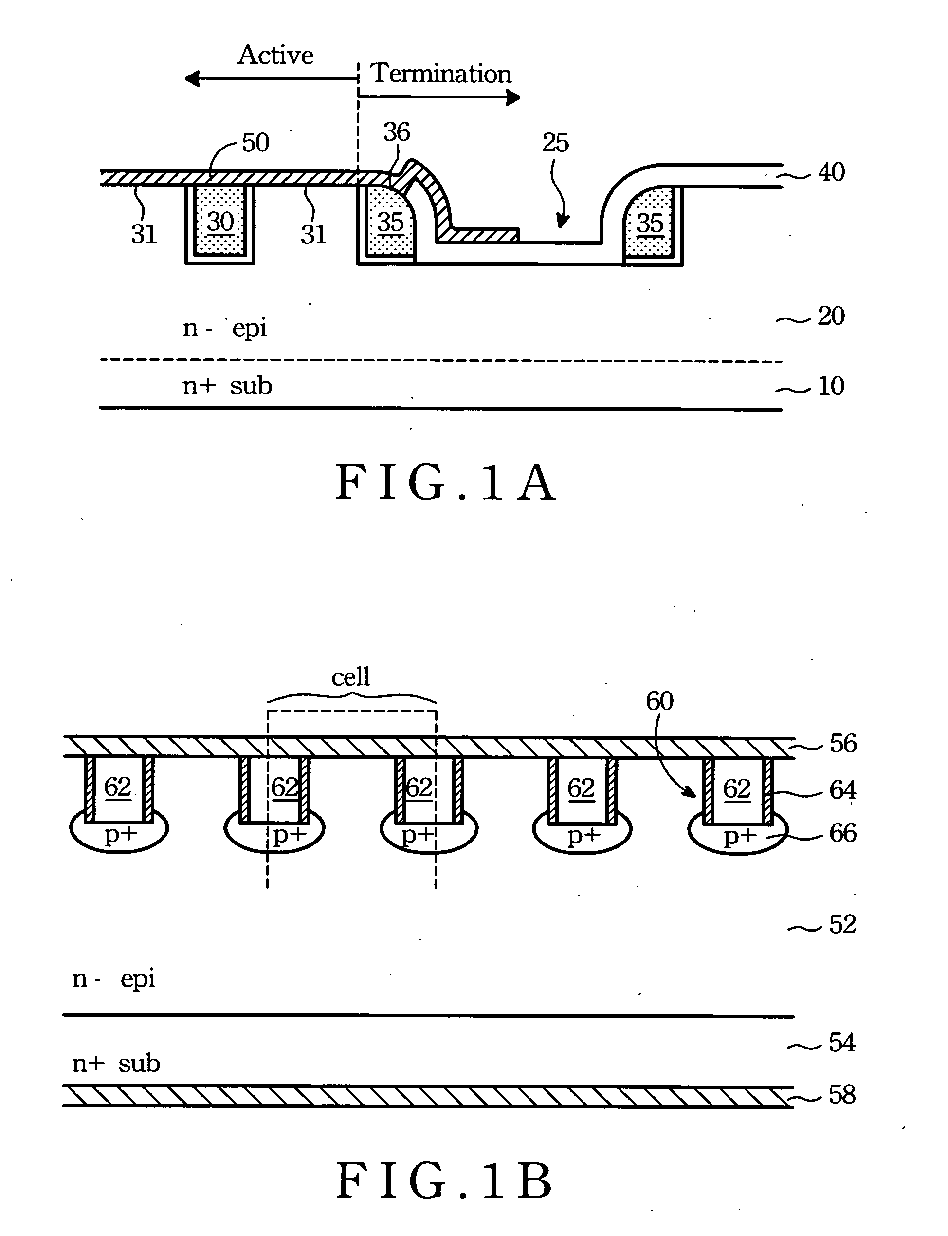
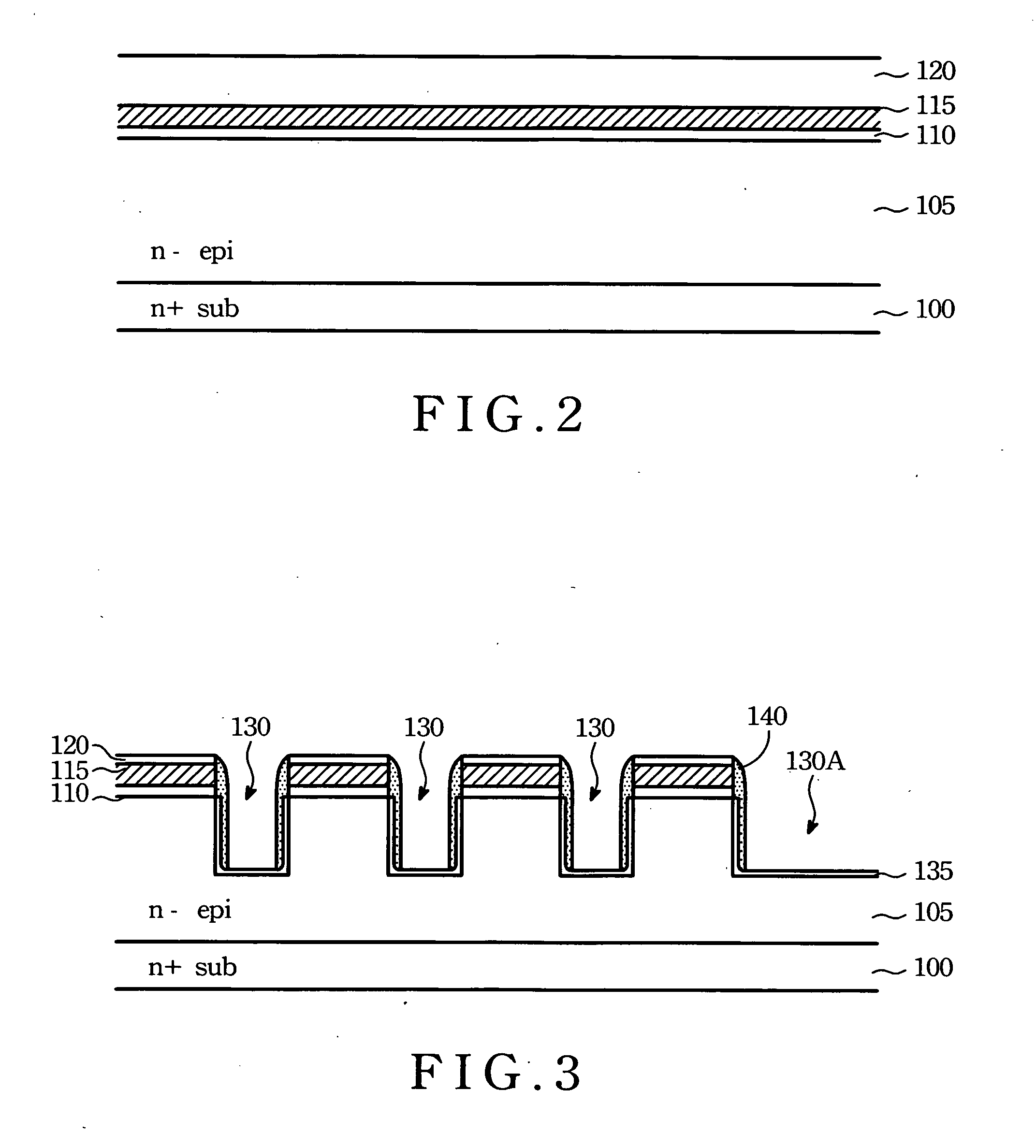
[0024]As depicted in the forgoing background of the invention, the conventional techniques requires at least three photo masks to form a power rectifier device and its termination structure. The present invention can simplify the processes and reduce the photo mask requirement to two. In addition, the structure of the invention proposed contains LOCOS at the bottom of the trenches, and hence, the structure is capable of tolerating high reverse biased voltage. The detailed descriptions are as follows:

[0025]Referring to FIG. 2, a cross-sectional view shows an n+ doped semiconductor substrate 100 thereof formed successively with an n− epi-layer 105, a first oxide layer 110, a first nitride layer (Nit 1) 115, and a second oxide layer 120. The first oxide layer 110 is formed of about 5-200 nm by a thermal oxidation or by a chemical vapor deposition (CVD). The nitride layer 115, and the second oxide layer 120 are formed by CVD to about 50-500 nm and 40-1000 nm, respectively, in thickness....


PUM


Abstract

A power Schottky rectifier device and method of making the same are disclosed. The Schottky rectifier device includes a LOCOS structure grown on the bottom of the trenches by using nitride spacer on the sidewall of the trenches as a thermal oxidation mask. A polycrystalline silicon layer is then filled the first trenches. Under LOCOS structure, a p doped region is optionally formed to minimize the current leakage when the device undergoes a reverse biased. A Schottky barrier silicide layer formed by sputtering and annealing steps is formed on the upper surfaces of the epi-layer and the polycrystalline silicon layer. A top metal layer served as anode is then formed on the Schottky barrier silicide layer and extended to cover a portion of field oxide region of the termination trench. A metal layer served as a cathode electrode is then formed on the backside surface of the substrate opposite to the top metal layer.

Description

FIELD OF THE INVENTION[0001]The present invention relates to a semiconductor process, specifically, to a novel termination structure for trench MOS devices so as to prevent leakage current.BACKGROUND OF THE INVENTION[0002]Schottky diode is an important power device and used extensively as output rectifiers in switching-mode power supplies and in other high-speed power switching applications, such as motor drives, switching of communication device, industry automation and electronic automation and so on. The power devices are usually required characteristics of carrying large forward current, high reverse-biased blocking voltage, such as above 100 volt, and minimizing the reverse-biased leakage current.[0003]A number of power rectifiers have been used to provide high current and reverse blocking characteristics. Hsu et al disclosed a Schottky rectifier structure in IEEE ELECTRON DEVICE LETTERS, vol. 22, No. 11, p. 531 (2001); “A Novel Trench Termination Design For 100 V TMBS diode Ap...

Claims


Application Information

Patent Timeline
IPC IPC(8): H01L23/58
CPCH01L29/66143H01L29/8725H01L29/872
Inventor WU, SHYE-LIN
Owner CHIP INTEGRATION TECH
Why Eureka
Try Eureka