Dual structure finfet and method of manufacturing the same

a technology of finfet and finfet, which is applied in the direction of transistors, electrical devices, semiconductor devices, etc., can solve the problems of complicated process that cannot be easily implemented, the integration density of a circuit is not significantly enhanced, and the enhancement density of integration is limited. to achieve the effect of enhancing the integration density of a circui

Active Publication Date: 2008-06-12
ELECTRONICS & TELECOMM RES INST
View PDF9 Cites 41 Cited by
  • Summary
  • Abstract
  • Description
  • Claims
  • Application Information

AI Technical Summary

Benefits of technology

[0010]The present invention is directed to a dual structure FinFET and a method of manufacturing the same, which forms a solid source material layer between an N-type FinFET and a P-type FinFET formed in a dual structure and defines source and drain regions through diffusion of the solid source material to enhance the density of integration of a circuit.
[0011]The present invention is also directed to a dual structure FinFET and a method of manufacturing the same, which forms an upper device of an epitaxial layer of silicon or silicon germanium to increase carrier mobility.

Problems solved by technology

However, in the horizontal type transistor 800 having the above-described configuration, the NMOS and PMOS are formed on the same plane, so that the integration density of a circuit is not significantly enhanced when the FinFET is configured even when actual sizes of devices are decreased.
Further, in the case of the PMOS, hole mobility is lower than electron mobility so that the width of the PMOS should be formed two to three times larger than the width of the NMOS in order to have the same level of current drivability as the NMOS, and the area of the FinFET actually becomes three to four times larger than the area of the NMOS layout, which thus causes a limit on enhancement of the density of integration.
Also, when a contact hole of the lower device is formed, an upper surface should be exposed and a portion of an interlayer dielectric layer should be left on a side surface of the contact hole, which requires a complicated process that cannot be easily implemented.

Method used


Image

  • Dual structure finfet and method of manufacturing the same
  • Dual structure finfet and method of manufacturing the same
  • Dual structure finfet and method of manufacturing the same

Examples


Embodiment Construction

[0030]The present invention will now be described more fully hereinafter with reference to the accompanying drawings, in which preferred embodiments of the invention are shown. This invention may, however, be embodied in different forms and should not be construed as limited to the embodiments set forth herein. Rather, these embodiments are provided so that this disclosure is thorough and complete and fully conveys the scope of the invention to those skilled in the art.

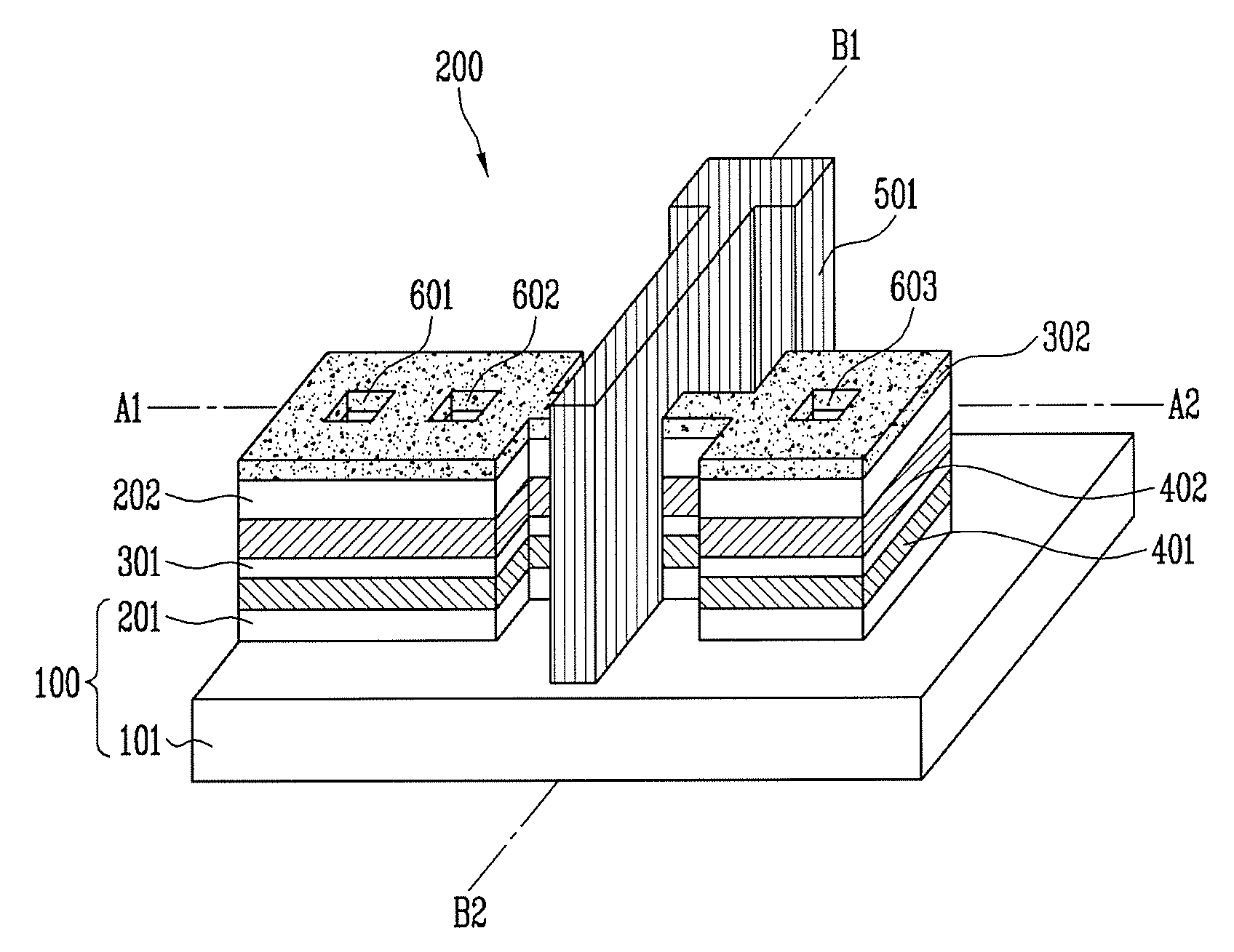
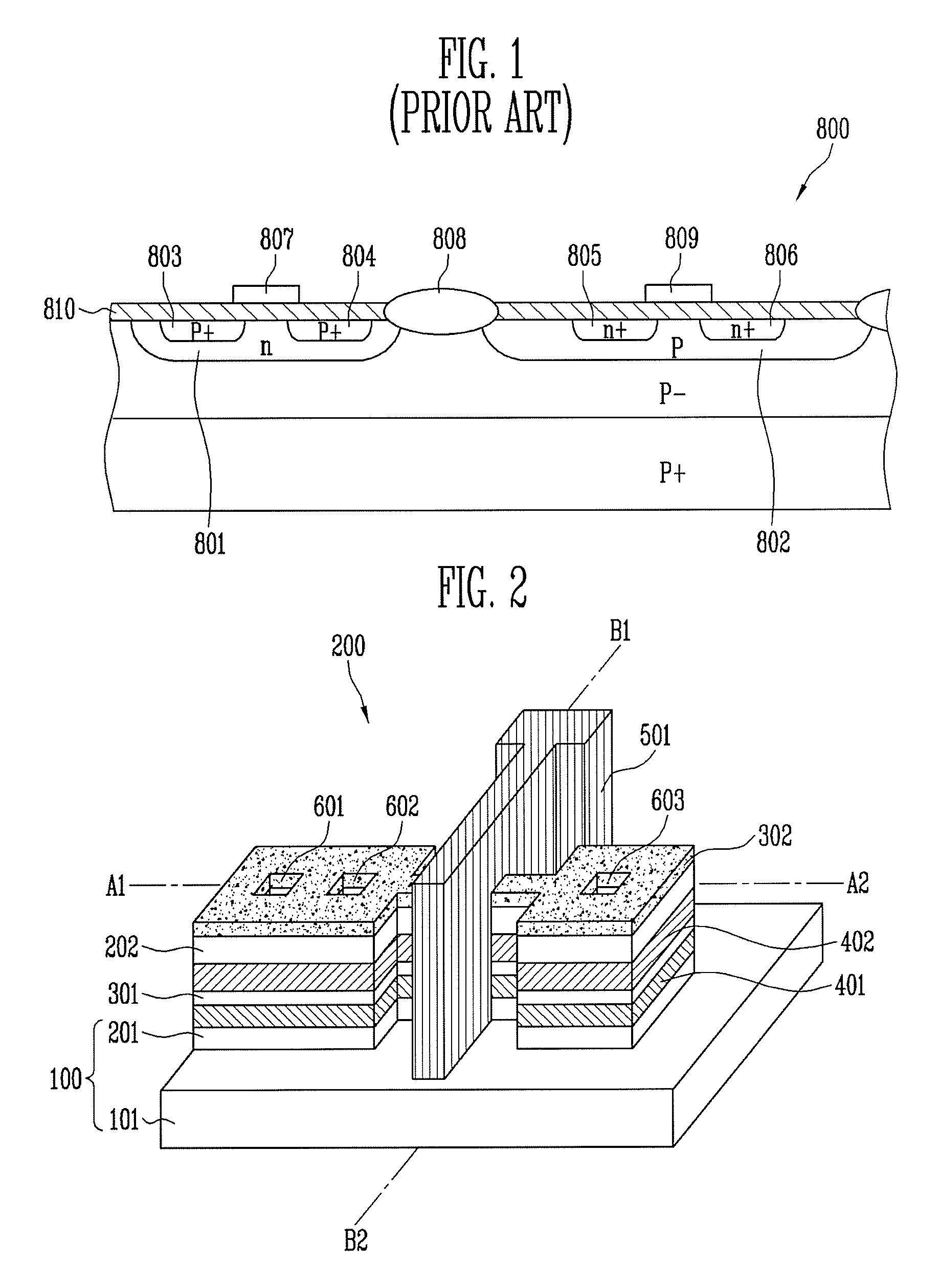
[0031]FIG. 2 is a partially enlarged perspective view of a dual structure FinFET according to a first embodiment of the present invention.

[0032]Referring to FIG. 2, a FinFET 200 according to the present invention includes a substrate 100 composed of an oxide layer 101 and a lower silicon layer 201 as a single crystalline silicon layer, a lower device having a gate electrode 501, an upper device formed above the lower device and having the gate electrode 501, first and second solid source material layers 401 and 402 fo...


PUM

PropertyMeasurementUnit
thicknessaaaaaaaaaa
lengthaaaaaaaaaa
gate lengthaaaaaaaaaa

Abstract

Provided are a dual structure FinFET and a method of fabricating the same. The FinFET includes: a lower device including a lower silicon layer formed on a substrate and a gate electrode vertically formed on the substrate; an upper device including an upper silicon layer formed on the lower device and the vertically formed gate electrode; and a first solid source material layer, a solid source material interlayer insulating layer, and a second solid source material layer sequentially formed between the lower silicon layer and the upper silicon layer. Therefore, the FinFET can be provided which enhances the density of integration of a circuit, suppresses thin film damages due to ion implantation using solid phase material layers, and has a stabilized characteristic by a simple and low-cost process. Also, mobility of an upper device can be improved to enhance current drivability of the upper device, isolation can be implemented through a buried oxide layer to reduce an effect due to a field oxide layer, and raised source and drain can be implemented to reduce serial resistance components of the source and drain to increase current drivability.

Description

CROSS-REFERENCE TO RELATED APPLICATION[0001]This application claims priority to and the benefit of Korean Patent Application No. 2006-123983, filed Dec. 7, 2006, the disclosure of which is incorporated herein by reference in its entirety.BACKGROUND[0002]1. Field of the Invention[0003]The present invention relates to a dual structure Fin Field Effect Transistor (FinFET) having a Fin channel and a method of manufacturing the same, and more particularly, to a FinFET having a dual structure where an N-type FinFET and a P-type FinFET which are formed of solid source material layers are stacked, and a method of manufacturing the same.[0004]The present invention has been produced from the work supported by the IT R&D program of MIC (Ministry of Information and Communication) / IITA (Institute for Information Technology Advancement) [2006-S006-01, Components / Module technology for Ubiquitous Terminals] in Korea.[0005]2. Discussion of Related Art[0006]As techniques of manufacturing semiconducto...

Claims


Application Information

Patent Timeline
Patent Type & Authority Applications(United States)
IPC IPC(8): H01L27/12H01L21/84
CPCH01L21/845H01L27/1211H01L29/7854H01L29/785H01L29/66795H01L29/41791
Inventor CHO, YOUNG KYUNROH, TAE MOONKIM, JONG DAE
Owner ELECTRONICS & TELECOMM RES INST
Why Eureka
Try Eureka