Method for non-contact testing of marginal integrated circuit connections

a technology of integrated circuits and connections, applied in the direction of electric connection testing, measurement devices, instruments, etc., can solve the problems of inability to test the ic device being tested, inability to use a single universal value of the stimulus voltage applied to all nodes under capacitive lead-frame test of the device, and inability to accurately test the capacitive lead-frame. the effect of resistive connections

Inactive Publication Date: 2007-11-13
AGILENT TECH INC
View PDF10 Cites 7 Cited by
  • Summary
  • Abstract
  • Description
  • Claims
  • Application Information

AI Technical Summary

Benefits of technology

[0021]In another embodiment, a method for optimizing test parameters specific to a semiconductor junction for use in a non-contact connectivity test by a semiconductor tester includes determining a stimulus voltage range corresponding to a measurable difference in capacitance within a measurement accuracy of the tester between a low resistance joint and a high resistance joint at a junction under test, selecting a stimulus voltage value within the stimulus voltage range such that the selected stimulus vo...

Problems solved by technology

The primary concern with turning on semiconductor junctions is damage to the IC device being tested due to excessive current.
Moreover, not all newer technologies will use a simple protection circuit as shown in FIG. 1 because changing input/output (IO) standards may require protection of even lower voltage logic due to higher energy levels.
Even though ESD protection circuits for newer technologies are not predictable, however, at the basic level they almost invariably consist of one or more semiconductor junctions that either explicitly or implicitly carry some of the same characteristics as a diode.
However, because advancements in semiconductor processing technology (shrinking geometries, changes in doping materials and doping concentrations, etc.) has lead to semiconductor junctions that turn on not at a single threshold voltage (or sharp knee), but rather semiconductor junctions that may be characterized by different jun...

Method used


Image

  • Method for non-contact testing of marginal integrated circuit connections
  • Method for non-contact testing of marginal integrated circuit connections
  • Method for non-contact testing of marginal integrated circuit connections

Examples


Embodiment Construction

[0043]For simplicity and illustrative purposes, the principles of the embodiments are described. Moreover, in the following detailed description, references are made to the accompanying figures, which illustrate specific embodiments. Electrical, mechanical, logical and structural changes may be made to the embodiments without departing from the spirit and scope of the embodiments.

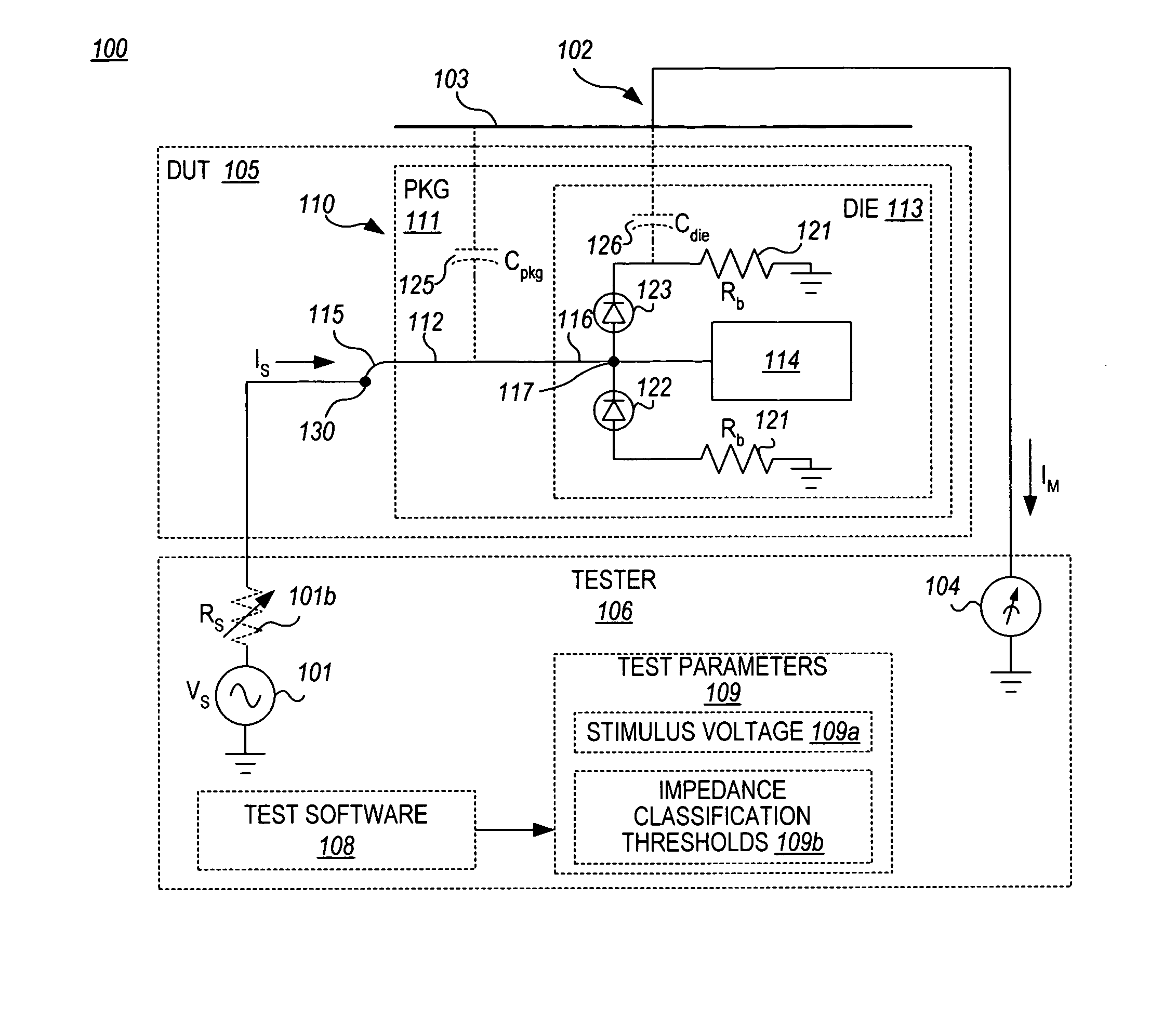
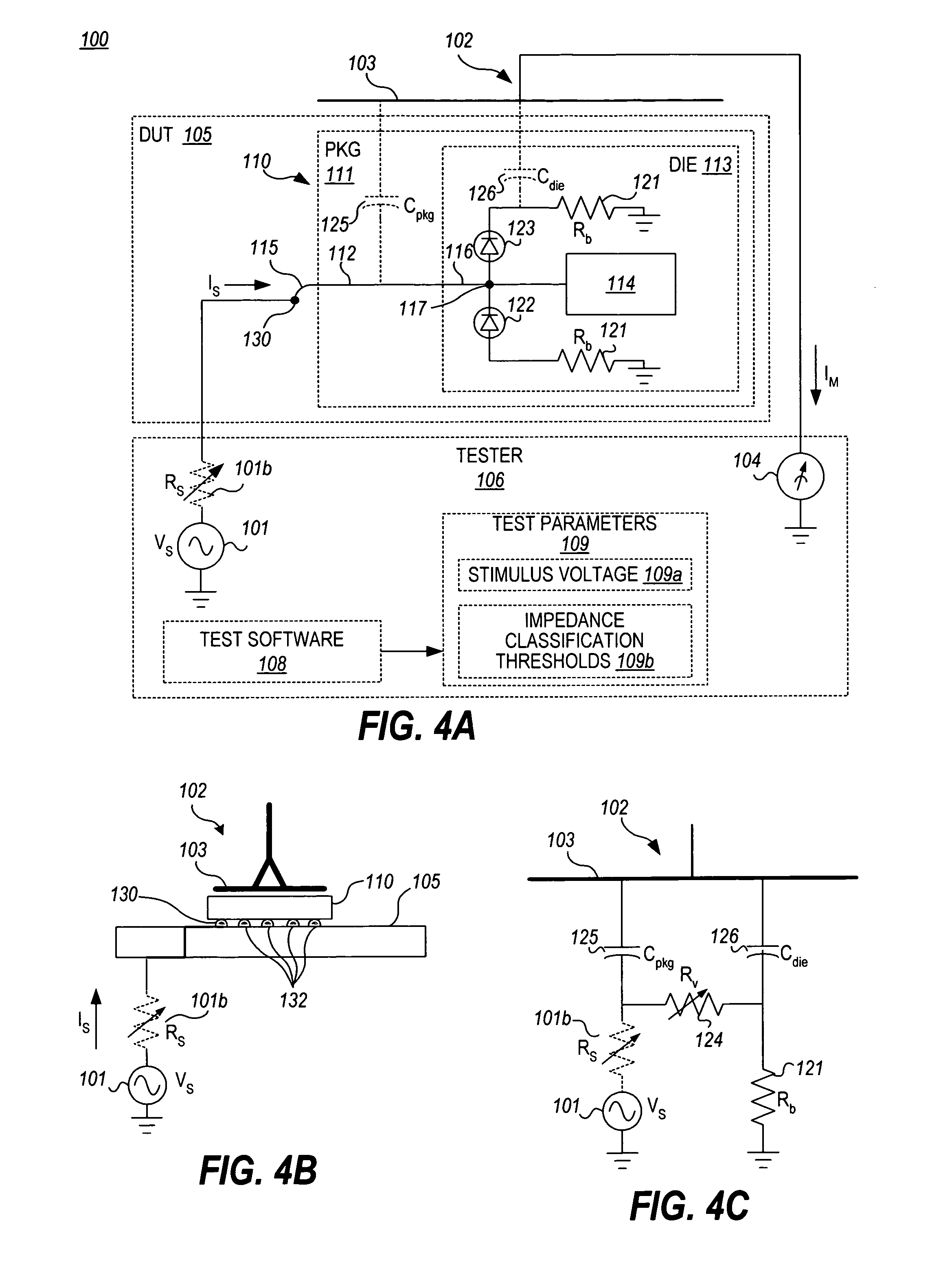
[0044]As used herein, the term “node” refers to the conductive portion of an electrical device that forms a single electrical point in the equivalent schematic diagram of the electrical device. For example, a node can be a pad of an integrated circuit die, a pin, a wire, a solder bump, or other interconnecting joint of an integrated circuit device, a pad or trace of a printed circuit board, an interconnecting joint of a component on the printed circuit board, or any combination thereof. For purposes of simplicity of description, whenever the term “node” is used in conjunction with a particular portion of an...


PUM


Abstract

Non-contact connectivity testing of joints connecting circuit junctions are improved through knowledge of characteristics of semiconductor junctions connected to component nodes of components of a device under test (DUT) to allow detection of high-impedance joints.

Description

BACKGROUND OF THE INVENTION[0001]Capacitive lead-frame sensing technologies are typically used to detect opens between an integrated circuit (IC) signal pin and a mounting substrate (e.g., a printed circuit board). The amplitude of the alternating current (AC) stimulus is normally set to a level that ensures that semiconductor junctions, from which the functional circuitry of the integrated circuit is formed, do not turn on. The primary concern with turning on semiconductor junctions is damage to the IC device being tested due to excessive current.[0002]When semiconductor junctions are turned on, the current supplied from the stimulus must be limited in magnitude and duration to prevent damage. The traditional semiconductor junction turns on at an AC stimulus of approximately 700 mV peak. Thus, the typical AC test stimulus for capacitive lead-frame technologies has been set around 200 mV, at which it is assumed that the junction current is insignificant to device damage and measurem...

Claims


Application Information

Patent Timeline
IPC IPC(8): G01R31/26G01R31/04
CPCG01R31/046G01R31/70
Inventor PARKER, KENNETH P.JACOBSEN, CHRIS R.NORRGARD, DAYTONSCHNEIDER, MYRON J.
Owner AGILENT TECH INC
Why Eureka
Try Eureka