Radiation-hardened transistor and integrated circuit

Active Publication Date: 2007-11-20
NAT TECH & ENG SOLUTIONS OF SANDIA LLC
View PDF17 Cites 48 Cited by
  • Summary
  • Abstract
  • Description
  • Claims
  • Application Information

AI Technical Summary

Problems solved by technology

As a result, the transient signal can change the state of a flip-flop, latch or memory cell formed by that transistor, thereby creating erroneous data in the IC and producing a single-event upset (SEU).
This scheme, which includes the use of replicated storage cells and voting schemes, can require a significant increase in circuit complexity.
This scheme has been effective for hardening against SETs which are generated external to the register, but can be ineffective for a SET produced inside the register.
As a result, this scheme is expected to become less effective for smaller and faster transistors, or else the operating frequency of the ICs will need to be limited to allow effective filtering of the SET signal.
This scheme imposes a space penalty due to the substrate space required for the feedba

Method used


Image

  • Radiation-hardened transistor and integrated circuit
  • Radiation-hardened transistor and integrated circuit
  • Radiation-hardened transistor and integrated circuit

Examples


Embodiment Construction

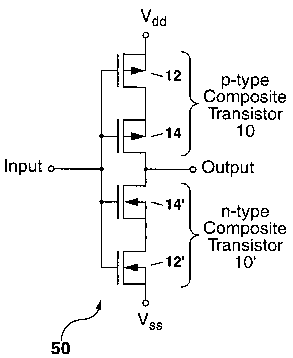
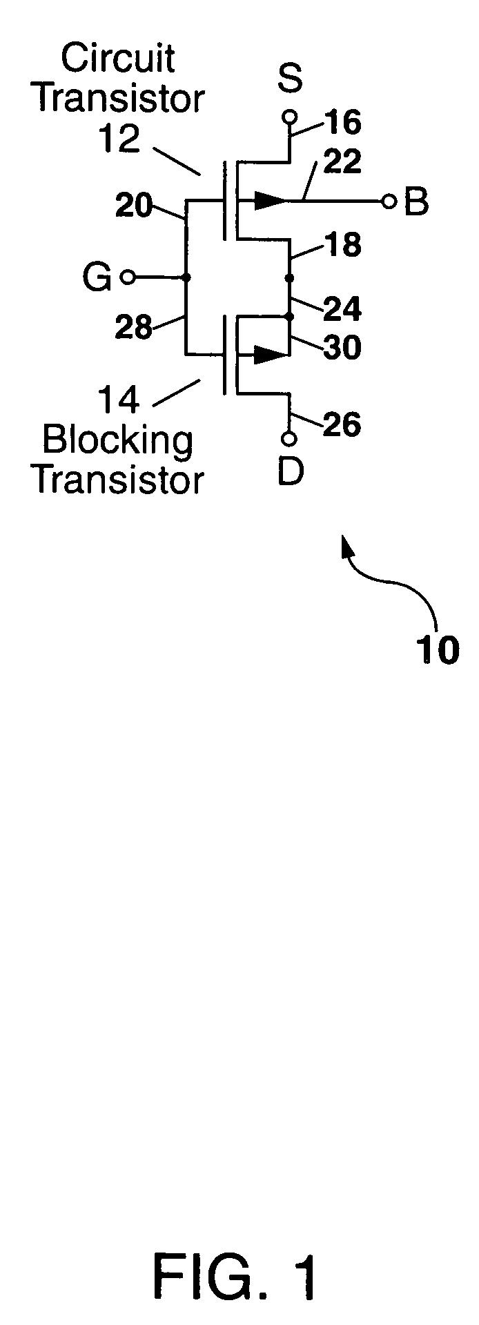
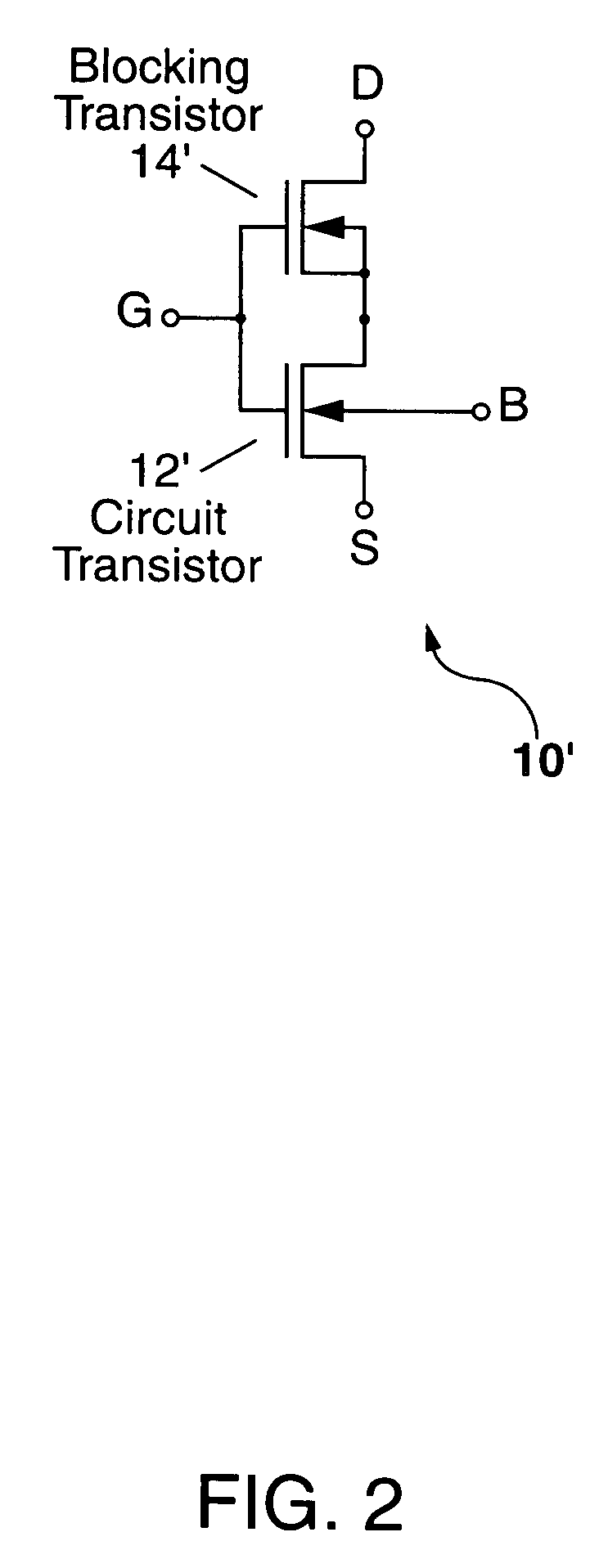
[0043]Referring to FIG. 1, there is shown a schematic diagram of a radiation-hardened composite transistor 10 of the present invention which can be used to form a radiation-hardened complementary metal-oxide semiconductor (CMOS) integrated circuit (IC). The composite transistor 10 comprises a circuit transistor 12 and a blocking transistor 14 connected together as shown. Each circuit transistor 12 and blocking transistor 14 can be a metal-oxide semiconductor (MOS) transistor. The term “MOS transistor” as used herein is intended to include transistors having gates formed of a metal, a metal alloy, or polycrystalline silicon (also termed polysilicon).

[0044]In the example of FIG. 1, the circuit transistor 12 further comprises a source terminal 16, a drain terminal 18, a gate terminal 20 and a body terminal 22. The blocking transistor comprises another source terminal 24, another drain terminal 26, another gate terminal 28 and another body terminal 30. The gate terminals 20 and 28 are c...


PUM


Abstract

A composite transistor is disclosed for use in radiation hardening a CMOS IC formed on an SOI or bulk semiconductor substrate. The composite transistor has a circuit transistor and a blocking transistor connected in series with a common gate connection. A body terminal of the blocking transistor is connected only to a source terminal thereof, and to no other connection point. The blocking transistor acts to prevent a single-event transient (SET) occurring in the circuit transistor from being coupled outside the composite transistor. Similarly, when a SET occurs in the blocking transistor, the circuit transistor prevents the SET from being coupled outside the composite transistor. N-type and P-type composite transistors can be used for each and every transistor in the CMOS IC to radiation harden the IC, and can be used to form inverters and transmission gates which are the building blocks of CMOS ICs.

Description

GOVERNMENT RIGHTS[0001]This invention was made with Government support under Contract No. DE-AC04-94AL85000 awarded by the U.S. Department of Energy. The Government has certain rights in the invention.FIELD OF THE INVENTION[0002]The present invention relates in general to radiation hardening of integrated circuits (ICs), and more particularly to a radiation-hardened composite transistor which can be used to radiation harden complementary metal-oxide semiconductor (CMOS) integrated circuits (ICs) to suppress single-event transients.BACKGROUND OF THE INVENTION[0003]Radiation hardening of ICs against single-event transients is becoming increasingly important as device sizes become smaller and smaller, and as clock speeds become faster and faster. A single-event transient (SET) is a disturbance in an IC produced by an energetic particle (e.g. an ion, proton, neutron) impinging on a sensitive node in the IC and depositing sufficient charge to create a transient signal therein. The sensit...

Claims


Application Information

Patent Timeline
IPC IPC(8): H01L23/62
CPCH01L23/556H03K19/00338H01L29/78H01L2924/3011H01L2924/0002H01L2924/00
Inventor MA, KWOK K.
Owner NAT TECH & ENG SOLUTIONS OF SANDIA LLC
Why Eureka
Try Eureka