Semiconductor storage apparatus

a technology of memory device and semiconductor, applied in the direction of information storage, static storage, digital storage, etc., can solve the problems of increasing power consumption at the time of writing, wasting current, and affecting the speed of writing, so as to achieve short time, shorten writing time, and improve writing speed

Active Publication Date: 2007-11-27
NEC CORP
View PDF13 Cites 9 Cited by
  • Summary
  • Abstract
  • Description
  • Claims
  • Application Information

AI Technical Summary

Benefits of technology

[0020]However, the mere use of the conventional constant current source is not enough to minimize the influence of the parasitic capacitor which depends upon the place of the selection array and let a write current flow in a short time. Further since the capacitance of the parasitic capacitor depends on the write current value, it has been difficult to minimize the influence of the parasitic capacitor according to the actual current value and let a write current flow in a short time. Furthermore, since there is a possibility that the actually accompanying parasitic capacitor will differ according to the chip, it is difficult to minimize the influence of the parasitic capacitor and let a write current flow in a short time.
[0021]An object of the present invention is to shorten the write speed and reduce the power consumption by preventing the parasitic capacitor from prolonging the time required until the write current reaches a predetermined value.
[0022]In order to achieve the object, a semiconductor memory device according to the present invention has a configuration in which the write current source path includes a circuit (hereafter referred to as a boost circuit) that stores electric charge at the time of write standby and instantaneously releases the electric charge at the time of write operation. By using the boost circuit, the parasitic capacitors which are present on the wire and the selector gate can be charged instantaneously. As a result, the amount of charging the parasitic capacitors with a current flowing from a constant current source circuit which is present separately from the boost circuit can be decreased. As a result, it becomes possible for the write current to rise in a short time. Consequently, writing can be conducted in a short time, and the increase of power consumption can be prevented.
[0024]In addition, in the boost circuit in the present semiconductor memory device, the boost capacitor is divided in order to form a geometric progression according to a selection pattern. Therefore, all boost capacitors are used at the time of maximum boost (writing to the remotest array, with maximum current). As a result, waste does not occur in the area occupied by the boost capacitor and the area occupied by the array can be increased.
[0036]In the semiconductor memory device according to the present invention, a time when storing charge in the boost circuit is set at a time after completion of an operation period of the constant current source. Therefore, the constant current source circuit can be made to operate stably. In its turn, an MRAM having a high process yield can be obtained.
[0038]According to the present invention, charging from the power supply to the capacitor is conducted at the time of standby, and discharge of the charge stored on the capacitor is conducted at the time of operation. As a result, charging the parasitic capacitors is conducted in a short time and the write time can be shortened. In general, values of these parasitic capacitors depend on the position of the write cell and current value. However, the parasitic capacitors can be charged at a suitable speed by adding a plurality of capacitor arrays and a capacitor selector for selecting a suitable capacitor to the write constant current source circuit. In other words, fast writing can be implemented. In particular, therefore, the present invention takes a great effect in implementing an MRAM having a large storage capacity.

Problems solved by technology

This results in a problem that power consumption at the time of writing increases.
Therefore, fast writing becomes difficult and a wasteful current is caused as represented by a shaded portion in FIG. 19B.
Especially in the case of the MRAM, therefore, there is a drawback that the power consumption increases because the write current value is large (several mA).
This problem becomes remarkable as the memory capacity becomes large. FIG. 20 is a block diagram showing a configuration used when currents are flowed through a large storage capacity array by using conventional constant current source circuits.

Method used


Image

  • Semiconductor storage apparatus
  • Semiconductor storage apparatus
  • Semiconductor storage apparatus

Examples


first embodiment

[0065]A semiconductor memory device according to the first embodiment of the present invention will now be described.

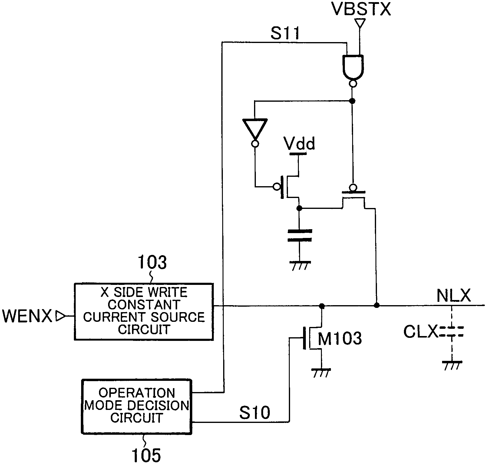
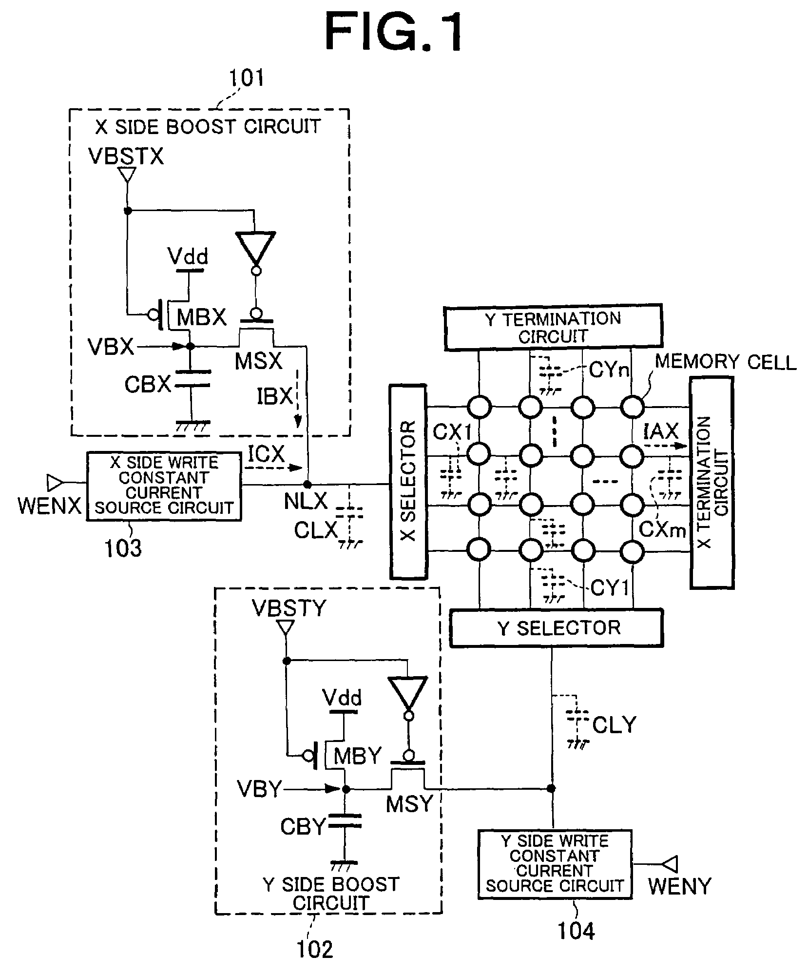
[0066]FIG. 1 is a block diagram showing a configuration of the semiconductor memory device according to the first embodiment of the present invention. In an X side boost circuit 101 shown in FIG. 1, one end of a boost capacitor CBX is connected to the ground and the other end thereof is connected to a PMOS transistor MSX and a PMOS transistor MBX via a terminal VBX. The other end of the PMOS transistor MBX is connected to a power supply voltage Vdd. At the time of boost standby (VBSTX=L level (GND)), the PMOS transistor MSX is in the off-state and the PMOS transistor MBX is in the on-state and consequently charge QB=CBX×Vdd is stored on the boost capacitor CBX. In a Y side boost circuit 102 as well, similar operation is conducted. Each of an X side write constant current circuit 103 and a Y side write constant current circuit 104 is a current source having a large out...

second embodiment

[0070]A semiconductor memory device according to the second embodiment of the present invention will now be described. The second embodiment aims at further shortening the write time by boosting the voltage applied to the boost capacitors CBX and CBY described in the first embodiment, thereby increasing the amount of charge that can be stored. Furthermore, according to the present circuit configuration, the amount of charge per unit area of capacitor stored on the boost capacitors CBX and CBY becomes large. This results in an advantage that the area of the boost capacitors CBX and CBY can be made small.

[0071]First, operation of the boost circuit will now be described with reference to FIG. 4A. It is supposed that the threshold voltage of a diode is Vt. At the time of standby, a potential at an input terminal A1 is V(A1)=0, a potential at an output terminal VBT is V(VBT)=Vdd−2Vt, and a potential at a node A2 is V(A2)=Vdd−Vt. If V(A1) is changed to V(A1)=Vdd in this state, the potenti...

third embodiment

[0077]A semiconductor memory device according to the third embodiment of the present invention will now be described.

[0078]In the third embodiment, a current boost circuit is applied to the large storage capacity array shown in FIG. 20. A write circuit diagram used in this embodiment is shown in FIG. 7. An X side current boost capacitor array 111 and an X side capacitor selector 112 are connected to X side main wire 113. AY side current boost capacitor array 114 and a Y side capacitor selector 115 are connected to Y side main wire 116. This is a feature of the third embodiment. Write switching between “0” and “1” is conducted by switching the Y side write current direction. In order to make it possible to add a boost current to the write current of both directions, capacitor arrays and capacitor selectors of two systems (represented as L and R) are prepared on the Y side. Since X side write operation is basically the same as the Y side write operation, only the X side writing will b...


PUM


Abstract

A semiconductor memory device in which information is written into a storage element by flowing current. The semiconductor memory device has a shortened write speed and reduced power consumption by preventing parasitic capacitors from prolonging the time required for a write current to reach a predetermined value. The semiconductor memory device includes storage elements for storing information, a constant current source for writing information into the storage element by flowing current, and a boost circuit for charging parasitic capacitors by a time when an amount of a current flowed by the constant current source reaches an amount of a current required to write information into the storage element, at a predetermined position related to the storage element.

Description

TECHNICAL FIELD[0001]The present invention relates to a semiconductor memory device in which information is written into a storage element by flowing current. In particular, the present invention relates to a semiconductor memory device in which information is written into a tunnel magnetoresistance element by a magnetic field generated by flowing current.BACKGROUND ART[0002]In recent years, demand for a memory having characteristics of nonvolatility, a large storage capacity, a low voltage operation and low power consumption is increasing as a result of rapid spread of portable telephone or the like. The MRAM (magnetic random access memory) is anticipated as a memory having these characteristics. A storage element of the MRAM includes a TMR (tunnel magnetoresistance) element. Each TMR element has, for example, a configuration as shown in FIG. 16. The TMR element is formed by successively stacking a fixed ferromagnetic layer (pin layer) 901, a tunnel insulation layer 902, and a free...

Claims


Application Information

Patent Timeline
Patent Type & Authority Patents(United States)
IPC IPC(8): G11C5/14G11C11/15
CPCG11C11/15
Inventor HONDA, TAKESHISAKIMURA, NOBORUSUGIBAYASHI, TADAHIKO
Owner NEC CORP
Why Eureka
Try Eureka