Electron-emitting apparatus

a technology of electron-emitting apparatus and electron-emitting tube, which is applied in the direction of instruments, discharge tube luminescnet screens, process and machine control, etc. it can solve the problems of reducing the color purity and contrast of images in display, unnecessary electron emission, and damage to the electron-emitting apparatus, so as to avoid excessive electron emission and suppress unnecessary electron emission

Inactive Publication Date: 2007-12-04
NGK INSULATORS LTD
View PDF14 Cites 3 Cited by
  • Summary
  • Abstract
  • Description
  • Claims
  • Application Information

AI Technical Summary

Benefits of technology

[0011]The present invention has been made based on these findings. It is one of objects of the present invention to avoid unnecessary electron emission by properly controlling the voltage and the like applied to the collector electrode. Since the collector electrode is arranged to oppose the upper electrode, unnecessary electron emission can be suppressed by controlling the voltage and the like applied to the collector electrode.
[0055]According to this structure, the collector voltage applying means requires only one switching element. Thus, the collector voltage applying means becomes inexpensive and achieves high reliability.

Problems solved by technology

Once such intense light emission occurs, emission of abnormally intense light may continue due to continuation of the plasma state.
Unnecessary electron emission decreases the color purity and the contrast of the images in the display.
Moreover, emission of abnormally intense light sometimes scatters the materials that constitute the upper electrode 14 and destroy the upper electrode 14, or even pierces holes in the emitter section 13, thereby damaging the electron-emitting apparatus.

Method used


Image

  • Electron-emitting apparatus
  • Electron-emitting apparatus
  • Electron-emitting apparatus

Examples


first embodiment

Structure

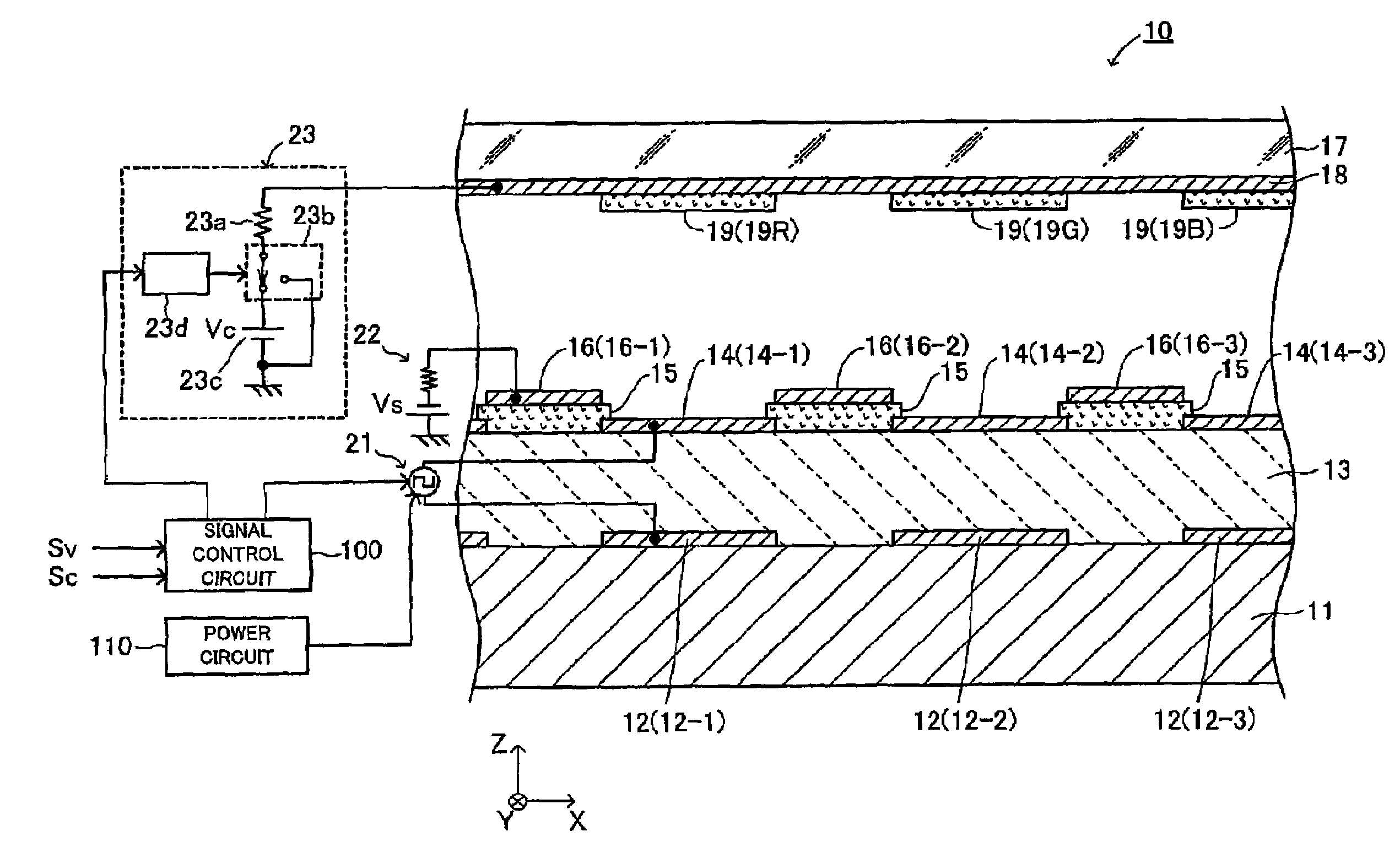
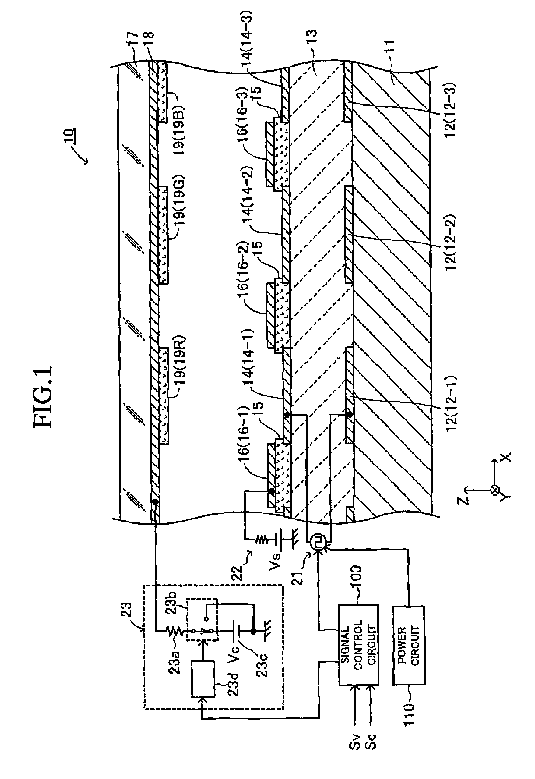
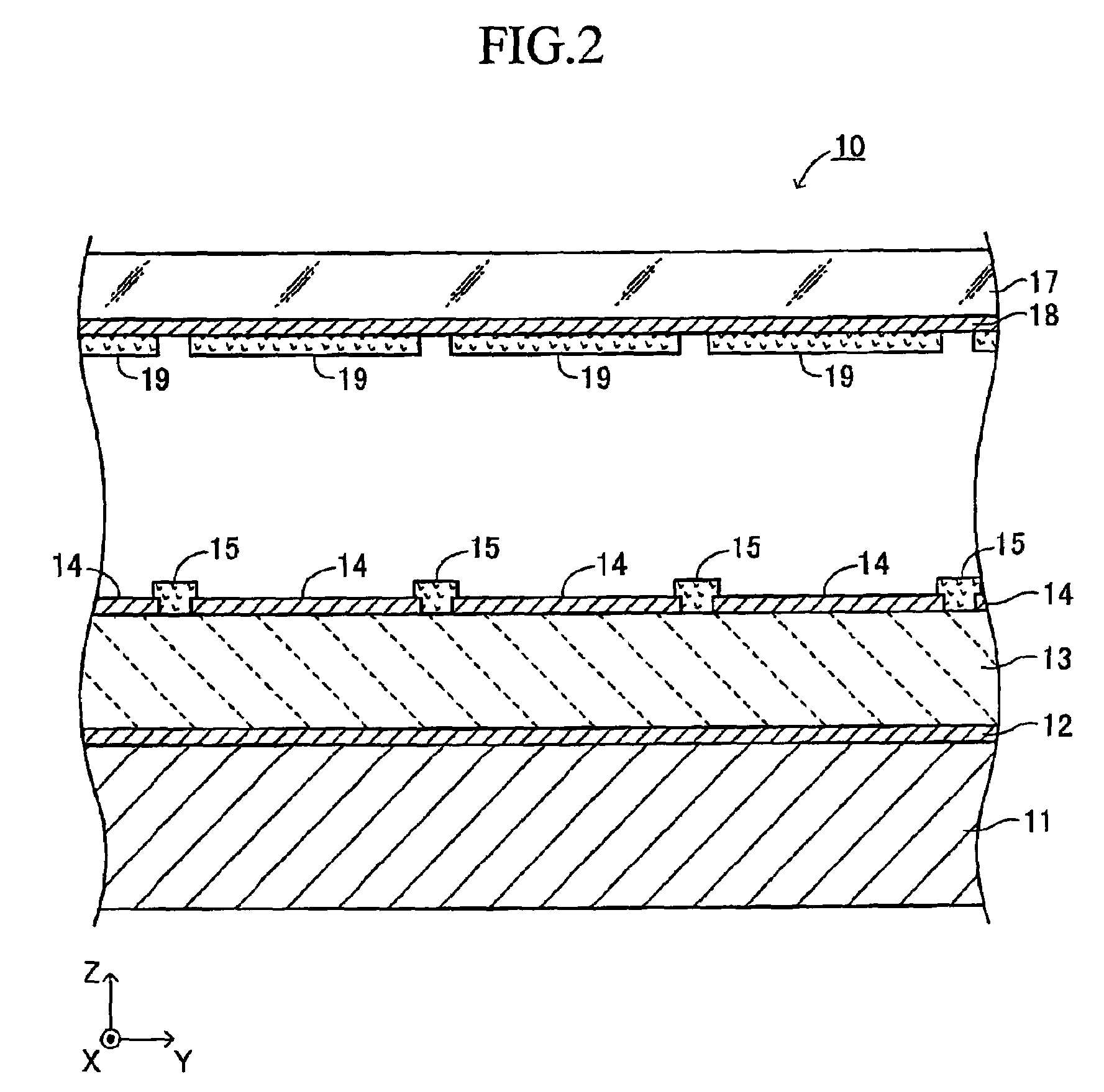
[0080]As shown in FIGS. 1 to 3, an electron emitting apparatus (an electron emitting device) 10 according to a first embodiment of the present invention includes a substrate 11, a plurality of lower electrodes (lower electrode layers) 12, an emitter section 13, a plurality of upper electrodes (upper electrode layers) 14, insulating layers 15, and focusing electrodes (focusing electrode layers, a bundling electrode to bundle emitted electrons) 16. FIG. 1 is a cross-sectional view of the electron emitting apparatus 10 taken along line I-I in FIG. 3, which is a partial plan view of the electron emitting apparatus 10. FIG. 2 is a cross-sectional view of the electron emitting apparatus 10 taken along line II-II in FIG. 3.

[0081]The substrate 11 is a thin plate having an upper surface and a lower surface parallel to the plane (X-Y plane) defined by the X axis and the Y axis perpendicular to each other. The thickness direction of the substrate 11 is the Z-axis direction perpendicul...

second embodiment

[0150]An electron-emitting apparatus according to a second embodiment of the present invention will now be described. The second embodiment differs from the first embodiment only in that the collector electrode ON time is set at a time point different from the collector electrode ON time of the first embodiment. Thus, the description below is mainly directed to this difference.

[0151]In the second embodiment, the collector electrode ON time is set at a fourth time point (4) (the time t11 represented by reference character B in FIG. 8) at which the interelectrode voltage (drive voltage) Vin is again set, after the electrons are emitted, at the positive predetermined voltage Vp. In detail, based on the signal fed from the signal control circuit 100, the collector voltage applying circuit 23 switches the switching point to which the fixed connection point of the switching element 23b is connected from the earthed switching point to the switching point connected to the constant voltage s...

third embodiment

[0155]An electron-emitting apparatus according to a third embodiment of the present invention will now be described. The third embodiment differs from the first embodiment only in that the collector electrode ON time is set to a time point different from the collector electrode ON time of the first embodiment. Thus, the description below is mainly directed to this difference.

[0156]In the third embodiment, the collector electrode ON time is set at a particular time within the period “starting from immediately after a fifth time point (5) (i.e., a time t12 in FIG. 8) at which the inrush current in the emitter section 13 becomes the maximum by again changing the interelectrode voltage (drive voltage) Vin to the positive predetermined voltage Vp” after the electron emission and “ending at a sixth time point (6) (i.e., a time t14) at which the polarization reversal (the positive-side polarization reversal) in the emitter section is substantially completed”.

[0157]Specifically, the switch ...


PUM


Abstract

An electron emitting apparatus includes a lower electrode, an emitter section made of a dielectric material, a plurality of upper electrodes having micro through holes, and a collector electrode opposing the upper electrodes. In this electron-emitting apparatus, electrons are accumulated in the emitter section by controlling the potential difference (drive voltage) between the lower and upper electrodes with respect to the potential of the lower electrode to a negative predetermined voltage. At this time, the collector electrode of the electron-emitting apparatus is grounded. Thus, unnecessary electron-emitting is suppressed. Subsequently, the drive voltage is changed to a positive predetermined voltage. As a result, polarization reversal occurs in the emitter section, and accumulated electros are emitted through the micro through holes in the upper electrodes by Coulomb repulsion. At this time, a positive voltage Vc is applied to the collector electrode to give large energy to accelerate the electrons.

Description

[0001]This application claims the benefit of Japanese Application No. 2004-286633, filed Sep. 30, 2004, the entirety of which is incorporated herein by reference.BACKGROUND OF THE INVENTION[0002]1. Field of the Invention[0003]The present invention relates to an electron-emitting apparatus including an emitter section made of a dielectric material, a lower electrode disposed below the emitter section, and an upper electrode disposed above the emitter section.[0004]2. Description of the Related Art[0005]In the related art, an electron-emitting apparatus including an emitter section made of a dielectric material, a lower electrode (lower electrode layer) disposed below the emitter section, and an upper electrode (upper electrode layer) disposed above the emitter section and having numerous micro trough holes has been known. According to this type of electron-emitting apparatus, a high-voltage pulse is applied between the upper electrode and the lower electrode to reverse the polarizati...

Claims


Application Information

Patent Timeline
Patent Type & Authority Patents(United States)
IPC IPC(8): G05F1/00
CPCB82Y10/00G09G3/22H01J1/30H01J1/312H01J1/32H01J31/127G09G2320/0238H01L2924/0002H01L2924/00
Inventor OHWADA, IWAOAKAO, TAKAYOSHIKAMEJI, TETSUYUKINAKAMURA, HIROKAZU
Owner NGK INSULATORS LTD
Why Eureka
Try Eureka