LDMOS transistor with improved gate shield

a gate shield and transistor technology, applied in the field of lateral diffusion mos transistors, can solve the problems of shield capacitance and high drain to source in the structure, and achieve the effect of reducing coupling capacitance and being easy to fabrica

Active Publication Date: 2007-12-11
F POSZAT HU
View PDF13 Cites 20 Cited by
  • Summary
  • Abstract
  • Description
  • Claims
  • Application Information

AI Technical Summary

Benefits of technology

[0008]In accordance with one embodiment of the present invention, a LDMOS transistor has a gate shield which is interconnected with the source contact but does not comprise the source contact metal. The shield structure is thin relative to the drain contact to thereby reduce coupling capacitance to the drain contact and with the shield structure extending to and contacting the source contact. The structure is readily fabricated using conventional semiconductor processing.
[0009]In accordance with another embodiment of the invention, planarity of the structure can be enhanced by plating the source, drain, and shield to different levels to realize a total planar structure.

Problems solved by technology

However, this structure has high drain to source and shield capacitance.

Method used


Image

  • LDMOS transistor with improved gate shield
  • LDMOS transistor with improved gate shield
  • LDMOS transistor with improved gate shield

Examples


Embodiment Construction

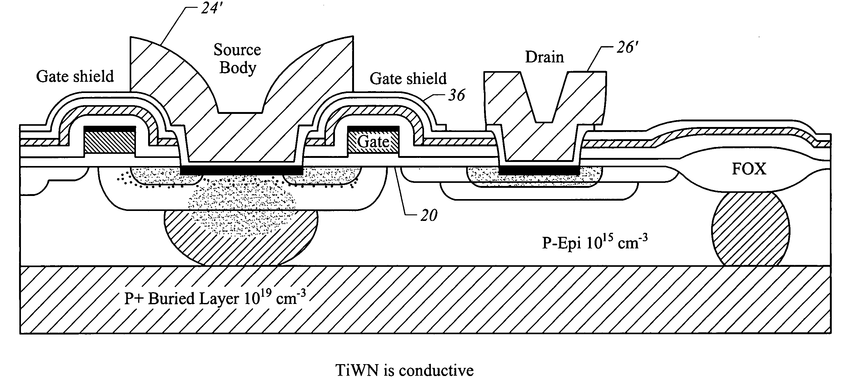
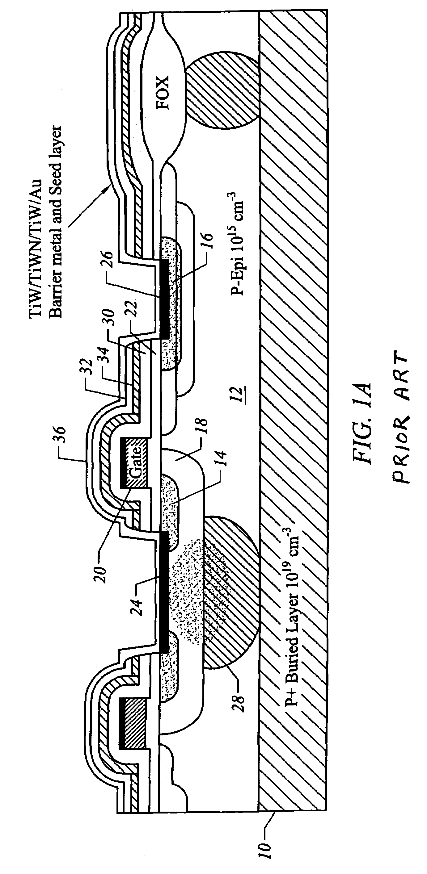
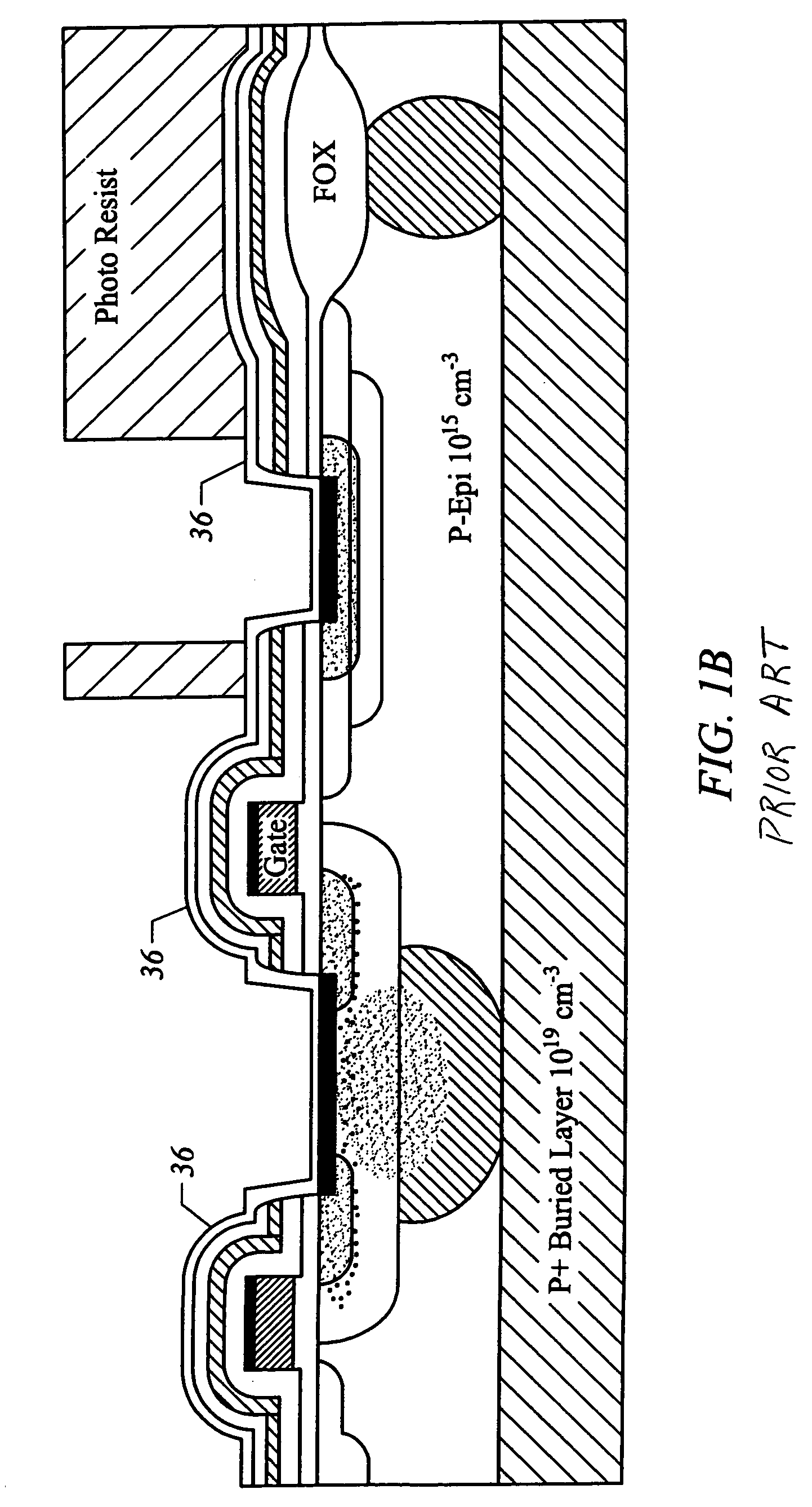
[0013]FIGS. 1A-1E are side views in section of the LDMOS transistor having a gate shield fabricated in accordance with prior art. The transistor is fabricated on a P+ substrate 10 which has a P− epitaxial layer 12 thereon. A source region 14 and drain region 16 are formed in a surface of epitaxial layer 12 with a P channel region 18 therebetween. Overlying channel 18 is a gate 20 which is insulated from channel 18 by gate dielectric 22, typically silicon oxide or silicon nitride. A source contact 24 is made to source 14 and also to an extension of P channel region 18, and a drain contact 26 is made to drain region 16. A P+ sinker layer 28 ohmically connects source contact 24 to P+ substrate 10.

[0014]Overlying gate 20 are silicon oxide layers 30, 32 and silicon nitride layer 34 which collectively provide insulation between conductive layer 36 and the underlying gate 20. Conductive layer 36 extends to source contact 24 and comprises titanium tungston / titanium tungston nitride / titanium...


PUM


Abstract

A LDMOS transistor having a gate shield provides reduced drain coupling to the gate shield and source by restricting the thickness of the gate shield and by confining a source contact to the source region without overlap of the gate.

Description

CROSS-REFERENCE TO RELATED APPLICATIONS[0001]This application is related to applications Ser. No. 10 / 870,012, filed Jun. 16, 2004, entitled LDMOS TRANSISTOR HAVING GATE SHIELD AND TRENCH SOURCE CAPACITOR, Ser. No. 10 / 870,720, filed Jun. 16, 2004, entitled LATERALLY DIFFUSED MOS TRANSISTOR HAVING N+ SOURCE CONTACT TO N-DOPED SUBSTRATE, and Ser. No. 10 / 870,795, filed Jun. 16, 2004, entitled LATERALLY DIFFUSED MOS TRANSISTOR HAVING INTEGRAL SOURCE CAPACITOR AND GATE SHIELD, all of which are incorporated herein by reference for all purposes.BACKGROUND OF THE INVENTION[0002]This invention relates generally to semiconductor transistors, and more particularly the invention relates to laterally diffused MOS (LDMOS) transistors.[0003]The LDMOS transistor is used in RF / microwave power amplifiers. The device is typically fabricated in an epitaxial silicon layer (P−) on a more highly doped silicon substrate (P+). A grounded source configuration is achieved by a deep P+ sinker diffusion from the...

Claims


Application Information

Patent Timeline
Patent Type & Authority Patents(United States)
IPC IPC(8): H01L29/76H01L21/336H01L29/10H01L29/40H01L29/417H01L29/45H01L29/78
CPCH01L29/402H01L29/7835H01L29/66659H01L29/1045H01L29/456H01L29/4175
Inventor BABCOCK, JEFFDARMAWAN, JOHAN AGUSMASON, JOHNDIEP, LY
Owner F POSZAT HU
Why Eureka
Try Eureka