Field emission display having gate plate

a technology of field emission and gate plate, which is applied in the direction of instruments, discharge tubes, luminescent screens, etc., can solve the problems of high voltage driving circuit, voltage that can be applied to the anode electrode, and control device failure, etc., and achieve the effect of reducing the driving voltage of the display row/column

Active Publication Date: 2007-12-18
ELECTRONICS & TELECOMM RES INST
View PDF30 Cites 9 Cited by
  • Summary
  • Abstract
  • Description
  • Claims
  • Application Information

AI Technical Summary

Benefits of technology

[0020]Accordingly, the present invention has been made in view of the above problems, and the present invention is directed to significantly re

Problems solved by technology

As a result, there is a disadvantage that an expensive high voltage driving circuit is required.
And, if the voltage is induced more than the breakdown voltage of the control devices 23, the control device could be failed.
Therefore, the conventional active-matrix field emission displa

Method used


Image

  • Field emission display having gate plate
  • Field emission display having gate plate
  • Field emission display having gate plate

Examples


Embodiment Construction

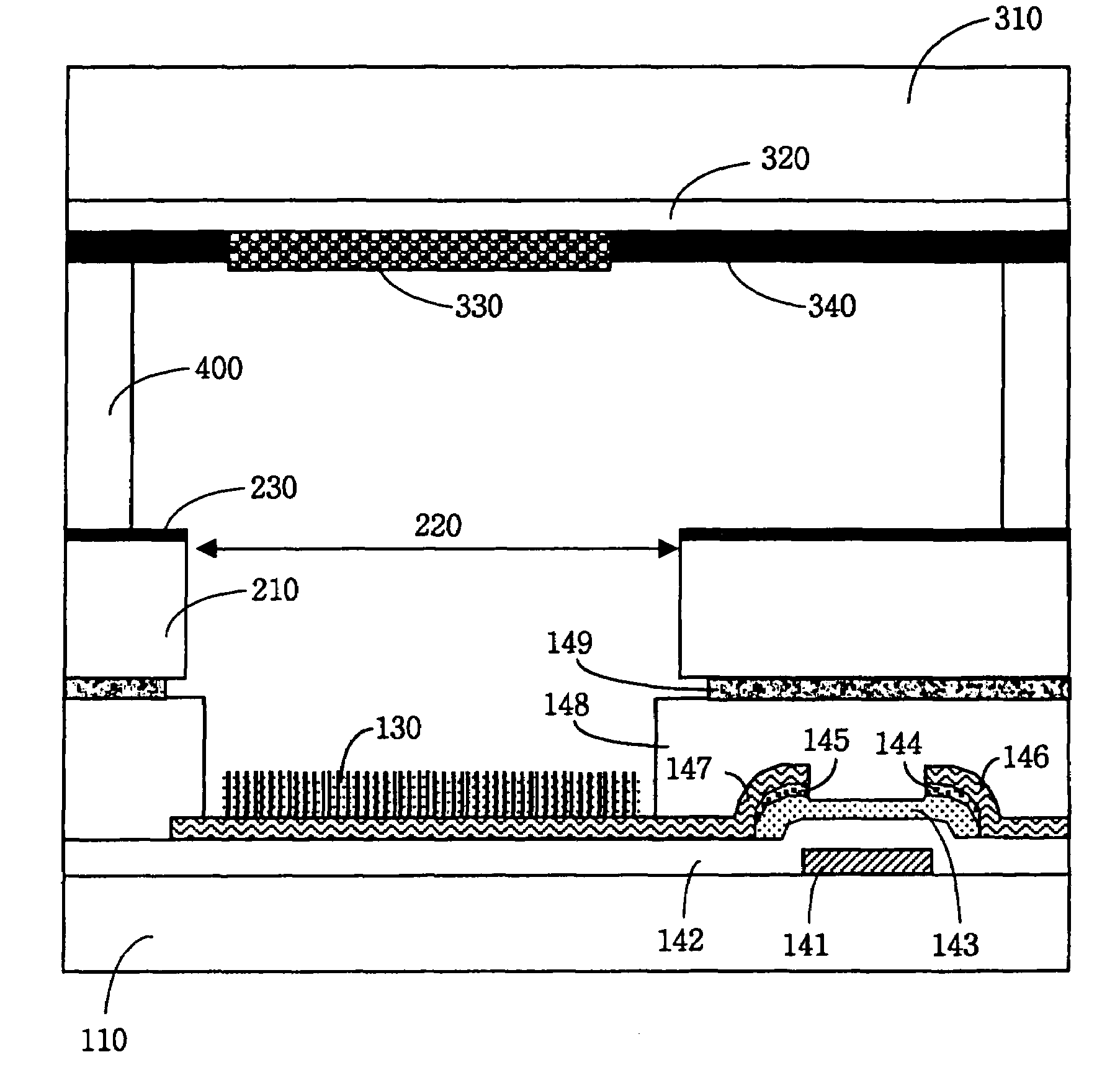
[0044]A field emission display of the present invention is significantly different comparing with that of the prior art field, in a cathode plate and the structure of a gate plate and a method of driving the same. Hereinafter, the field emission display according to the present invention will be described in detail with reference to FIG. 3 to FIG. 8.

[0045]FIG. 3 is a perspective view schematically illustrating a construction of an active-matrix field emission display having a gate plate according to the present invention and FIG. 4 is a perspective view schematically illustrating a cathode plate, a gate plate and an anode plate in a field emission display according to the present invention. The field emission display includes the cathode plate 100, the gate plate 200 and the anode plate 300.

[0046]As shown in FIG. 4, the cathode plate 100 includes a belt shaped row signal line 120S and column signal line 120D on an insulating substrate 110 including glass, plastic, various ceramics, ...


PUM


Abstract

The present invention relates to a field emission display in which a gate plate having a gate hole and a gate electrode around the gate hole is formed between an anode plate having phosphor and a cathode plate having a field emitter and a control device for controlling field emission current, wherein the field emitter of the cathode plate is constructed to be opposite to the phosphor of the anode plate through the gate hole.
According to the present invention, it is possible to significantly reduce the display row/column driving voltage by applying scan and data signals of the field emission display to the control device of each pixel, And the present invention is directed to improve the brightness of the field emission display in such a manner that the electric field necessary for field emission is applied through the gate electrode of the gate plate to freely control the distance between the anode plate and the cathode plate, so that a high voltage can be applied to the anode.

Description

BACKGROUND OF THE INVENTION[0001]1. Field of the Invention[0002]The present invention relates to a field emission display (FED) in which the field emission device is applied to a flat display, and in particular, to the field emission display in which a gate plate having a gate hole and a gate electrode around the gate hole is formed between an anode plate having phosphor and a cathode plate having a field emitter and a control device for controlling field emission current, wherein the field emitter of the cathode plate is constructed to be opposite to the phosphor of the anode plate through the gate hole.[0003]2. Background of the Related Art[0004]A field emission display is a device representing an image through cathodeluminescence of a phosphor, by colliding electron emitted from the field emitter of a cathode plate against the phosphor of an anode plate, wherein the cathode plate having the field emitter and the anode plate with the phosphor are formed to be opposite to each othe...

Claims


Application Information

Patent Timeline
IPC IPC(8): H01J1/62H01J29/04G09G3/20G09G3/22H01J29/02H01J29/32H01J29/46H01J29/48H01J29/87H01J29/96H01J31/12H01J63/04
CPCH01J29/028H01J29/467H01J31/127H01J29/481H01J2329/8625
Inventor SONG, YOON HOHWANG, CHI SUNCHUNG, CHOONG HEUILEE, JIN HO
Owner ELECTRONICS & TELECOMM RES INST
Why Eureka
Try Eureka