Memory device and sense amplifier circuit with faster sensing speed and improved insensitivities to fabrication process variations

Active Publication Date: 2008-01-08
AVAGO TECH INT SALES PTE LTD
View PDF2 Cites 13 Cited by
  • Summary
  • Abstract
  • Description
  • Claims
  • Application Information

AI Technical Summary

Benefits of technology

[0020]In some cases, the charging portion may include at least two p-channel transistors with source-to-drain paths coupled in series between the power supply voltage and the match line. For example, a first one of the p-channel transistors may be a switch activated by an enable signal supplied to the sense amplifier circuits, and the second one of the p-channel transistors may be a mirror device coupled for receiving the reference voltage from the reference generator. In such a case, the reference generator may be configured for detecting a maximum amount of current that is able to pass through the drain-to-source path of the pair of serially-connected n-channel transistors within the duplicate compare stack, and for generating a proportional reference voltage in response thereto. A p-channel reference device within the reference generator may then be used for supplying the reference voltage to the second p-channel transistor within the charging portion, where it is converted into a current to be supplied to the match line. In this manner, the converted current may be substantially equal to the maximum amount of current detected by the reference generator. This eliminates functional failures by ensuring that the converted current can pass through a single compare stack during

Problems solved by technology

In the particular case of CAM devices, sensing operations can consume a considerable amount of current (and hence power), as such operations typically involve the continuous charging of multiple match lines, and the sub

Method used


Image

  • Memory device and sense amplifier circuit with faster sensing speed and improved insensitivities to fabrication process variations
  • Memory device and sense amplifier circuit with faster sensing speed and improved insensitivities to fabrication process variations
  • Memory device and sense amplifier circuit with faster sensing speed and improved insensitivities to fabrication process variations

Examples


Embodiment Construction

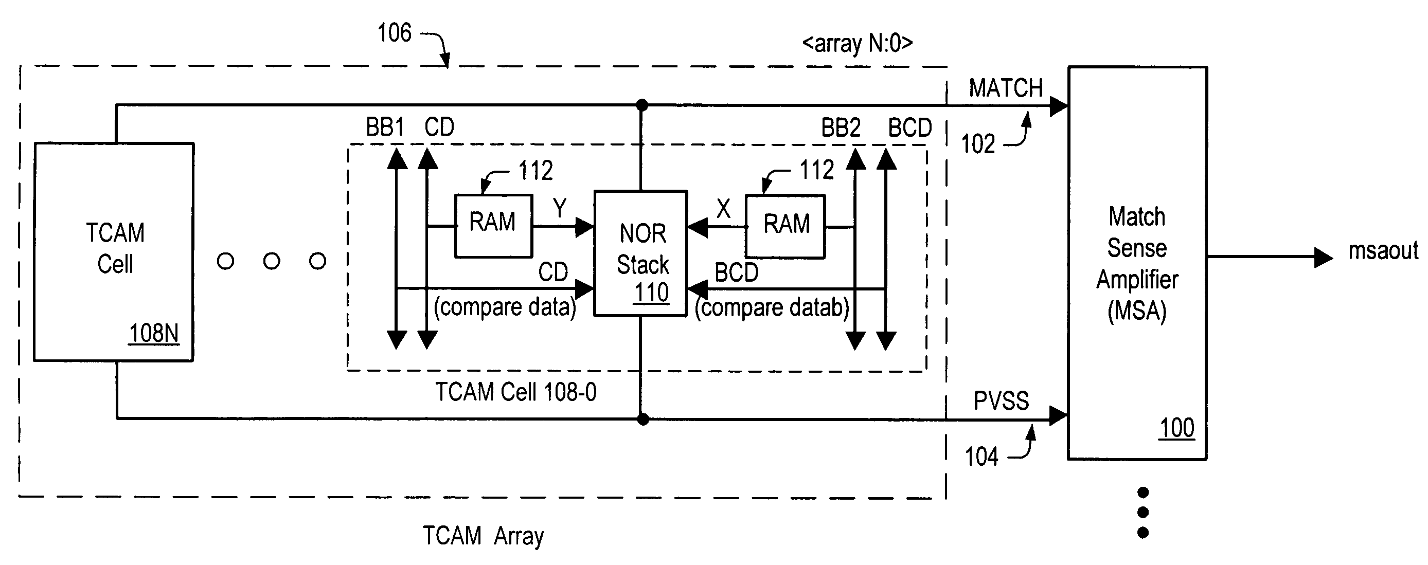
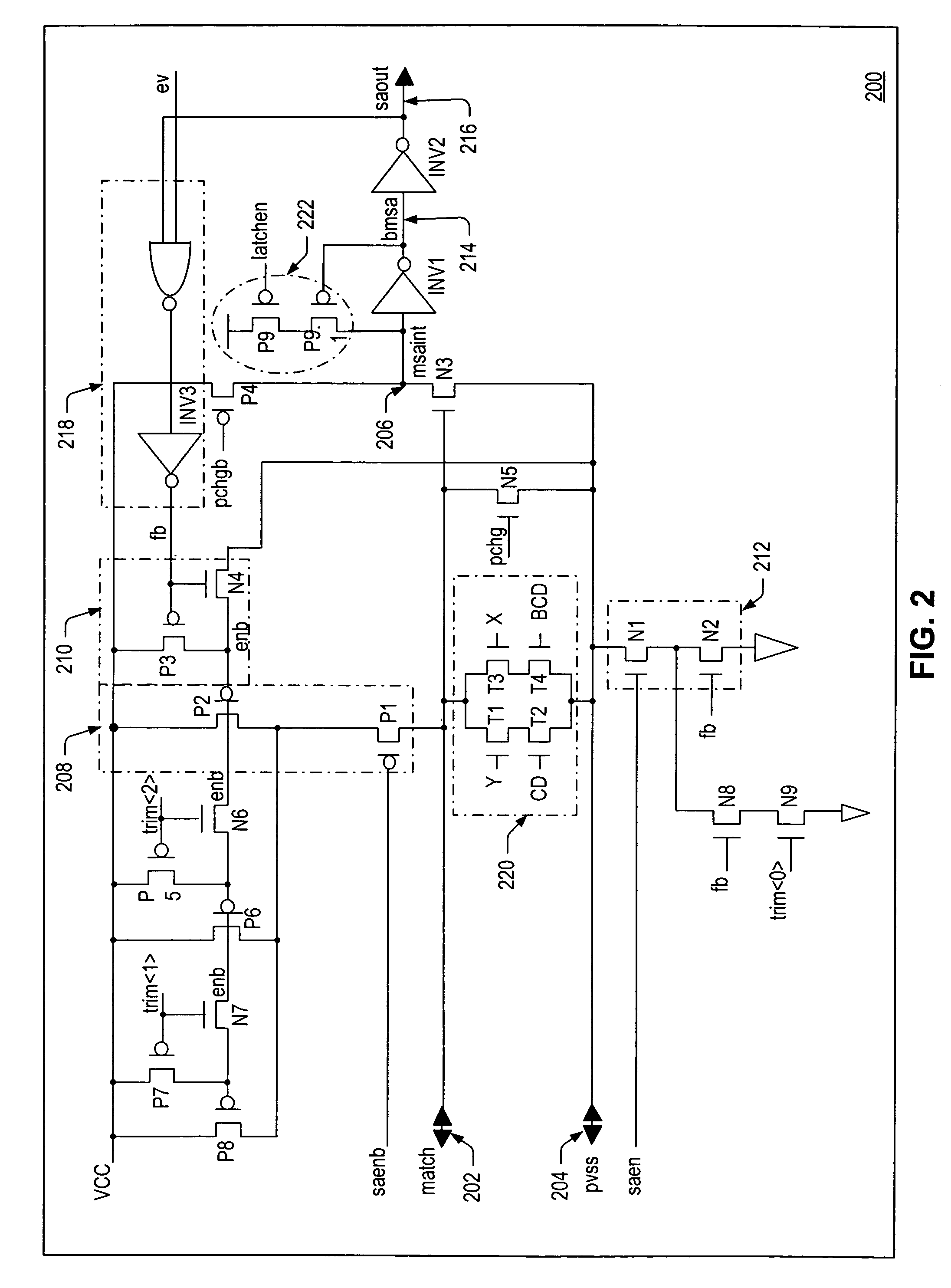
[0047]To reduce overall current consumption, a sense amplifier circuit may operate in conjunction with a “pseudo-supply” arrangement. A pseudo-VSS arrangement can include a pseudo-VSS node that is preset (i.e., pre-discharged) to a predetermined value (e.g., VSS). As will be described in more detail below, such an arrangement utilizes a charge sharing mechanism that functions to conserve charge on a match line, thus reducing overall current consumption in the sense amplifier circuit.

[0048]Various examples of a content addressable memory (CAM) including a pseudo-VSS arrangement are shown in U.S. Pat. No. 6,515,884 to Sywyk et al. U.S. Pat. No. 6,515,884 shares a common assignee with the present invention and is incorporated herein in its entirety. However, the examples disclosed in U.S. Pat. No. 6,515,884 should not be construed as limiting to the present invention.

[0049]FIG. 1 shows a memory architecture including a CAM device and a single-ended sense amplifier with a pseudo-VSS arr...


PUM


Abstract

A sense amplifier circuit with faster sensing speed and improved insensitivities to fabrication process variations (i.e., eliminated functional failures) is provided herein. According to one embodiment, the sense amplifier circuit associated with a row of memory cells within a memory device may include a charging portion, which is coupled for receiving a reference voltage that is supplied to at least one additional sense amplifier circuit within the memory device. The reference voltage is provided by a current reference generator, which is coupled to the sense amplifier circuit(s) for detecting: (i) a maximum amount of current that can pass through one compare stack within the memory cell array, or (ii) a difference between the maximum amount of current and the current contribution of an n-channel current source within the sense amplifier circuit. A memory device and method of operating one embodiment of the improved sense amplifier circuit are also provided herein.

Description

BACKGROUND OF THE INVENTION[0001]1. Field of the Invention[0002]This invention relates to sense amplifier circuits and, more particularly, to sense amplifier circuits with reduced power consumption, improved insensitivity to wafer process variations and faster sensing speed.[0003]2. Description of the Related Art[0004]The following descriptions and examples are given as background only.[0005]Sense amplifiers are commonly used in memory devices, such as random access memories (RAMs), read only memories (ROMs), and more specialized memories, such as content addressable memories (CAMs).[0006]Continuing goals for nearly all integrated circuits include lower power consumption, higher operating speeds, and lower operating voltages. In the particular case of CAM devices, sensing operations can consume a considerable amount of current (and hence power), as such operations typically involve the continuous charging of multiple match lines, and the subsequent discharging of select match lines....

Claims


Application Information

Patent Timeline
IPC IPC(8): G11C15/00
CPCG11C7/067G11C15/04
Inventor MENG, ANITA X.
Owner AVAGO TECH INT SALES PTE LTD
Why Eureka
Try Eureka